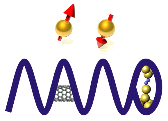
|
BMe Research Grant |

|
As submitted in October 2010
Faculty of Natural Sciences
Institute of Physics
Nanophysics
Introducing the research area
The physics of nanostructures created by novel technologies, beyond their fundamental importance in basic research, also raise the possibilities for promising industrial applications. Shrinking dimensions give rise to new type of behavior radically different from common macroscopic features: simple materials may realize unexpected functions on the nanoscale. A wide range of recent discoveries may serve technological development, including carbon and semiconductor nanostructures and a big variety of “bottom-up” self organizing nanoscale systems or the nanofabrication of devices from special materials. Some of the novel conceptions have already found their application in specific electronic devices.
Brief introduction of the research place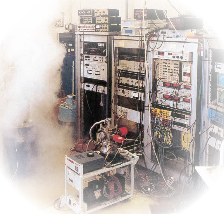
Understanding the nanoscale phenomena is not merely a challenge for theoretical research, but gives motivation for the development of novel experimental techniques at the same time. The scientific workshop is a community of theoretical and experimental researchers working on specific topics of nanoscience at the Institute of Physics. The scientific background is provided by the solid state physics school, a major contributor to the education of physicists at BUTE, the graduate school of physics working to high standards and a young research team with international experience. Of the several grants supporting research, OTKA spintronics project and two recently awarded young researcher ERC startup grants (CooPairEnt and Sylo) should be highlighted.
History and context of the research
Nanoscale materials have triggered a revolutionary development in several fields of science and technology, including space research, medicine and nanoelectronics. Successful applications, however, should build on the solid understanding of the underlying physical phenomena.
A
somewhat larger length scale is represented by the widely studied carbon
nanostructures (fullerene, nanotube, graphene). Our special focus is
put on
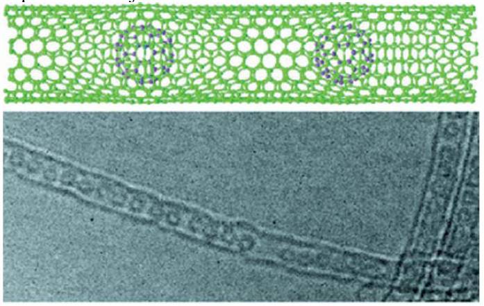 modifying the properties of single wall carbon nanotubes
by introducing various species of fullerene-based molecules into the
nanotube [4,5]. The figure to the right illustrates the arrangement of the
football-shaped fullerenes inside the carbon nanotubes. Below is an
electron microscope image with a magnification of 5 million.
A third level is defined by the artificially fabricated metal, semiconductor, superconductor hybrid devices, where nanostructure properties can be designed on a broad scale based on properly chosen materials. The submicron lateral structuring of hybrid nanostructures is provided by the equipments of the Nanotechnology laboratory.

Additionally
to the charge of the electrons, their internal rotation, i.e. their
“spin” also plays a fundamental role in nanoelectronics. Magnetic
behavior of materials is related to the magnetic moments of the
“spinning” electrons, whereas pairs of oppositely spinning electrons
(Cooper pairs) are responsible for superconductivity.
In nanoscale objects, phase information has an important role during the wave-like propagation of electrons, the spin can be preserved, and quantum phenomena are becoming dominant in the behavior of the system. This opens a possibility of using the spin of the electrons for information storage and transfer (spintronics), performing arithmetic operations on a quantum mechanical basis (qubit), or constructing transistors, memories and ultra-sensitive sensors based on the manipulation of a few atoms or single molecules (molecular electronics). These fields of modern physics play a central role in the theoretical and experimental research and technological developments of the scientific workshop.
Aim of the research
Our goal is the development and detailed experimental / theoretical study of such novel nanostructures, where understanding of nanoscale phenomena is not merely a challenge of fundamental research, but also carries the potential for later technological applications. In a range from atomic sizes to a few hundred nanometers, we not only apply the standard processes of modern nanotechnology (nanolithography, atomic layer deposition, chemical preparation) but also search for custom preparation techniques for contacting single molecules, creating self-organized structures or building atomic-scale switches.
The nanostructures are characterized by self-developed
scanning probe techniques, spectroscopic methods, electronic and
magnetic measurements. A highlighted topic of our experimental studies
is the investigation of spin-dependent phenomena:
i., detection and manipulation of nanoscale magnetic
domains by spin-polarized current,
ii., measurement of spin-diffusion by ESR and Andreev
spectroscopy,
iii., study of phase-, spin-, and superconducting
correlations in nanostructures (nanowires, graphene).
The two opposite spin electrons of a Cooper pair can be a
natural source for creating entangled electron pairs. Their
investigation is touching such fundamental questions of quantum
mechanics like the Einstein-Podolsky-Rosen paradox. The experimental
identification of entangled electrons split from a Cooper pair has a
fundamental importance in basic research, but it is also an essential
step towards the establishment of qubits, the basic units of envisioned
quantum computers at the same time.
Another important direction of our research is the development of reliable contacting techniques for single molecules applying self-designed break junction setups. Despite successes in recent activities in the field of molecular electronics, reliable and reproducible creation of molecular nanostructures is still an especially hard task, as – unlike pre-designed engineering of devices – it depends on the fine details of nanoscale chemical interactions and self-assembling properties. Therefore, detailed studies on the behavior of molecular nanostructures and comprehensive understanding of some reference systems have a fundamental role in the development of functional molecular electronic devices.
Methods
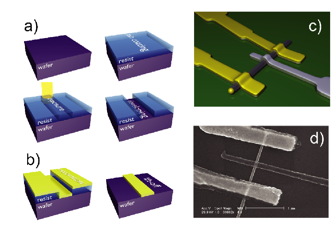 To create pre-designed nanostructures, electron-beam
lithography (EBL) is the most effective method. The principle of EBL:
(a) A thin polymer layer is scanned by an electron beam. The irradiated
regions can be removed by chemical processing, forming a mask for
evaporation. (b) Metal is evaporated on the mask, and the remainder of
the PMMA is removed. With these steps, complex metallic nanostructures
can be produced down to the range of 40–100 nm. EBL can also be applied
to contact pre-deposited nanoscale objects (e.g. semiconducting
nanowires, carbon nanotubes, graphene) by metallic electrodes. Plan and
realization of a nanocircuit from InAs nanowire are presented in figure
(c)/(d).
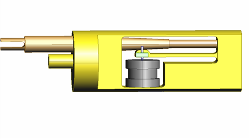
For the creation of nanoscale junctions, a widely applied
method is touching the investigated sample by the tip of a scanning
tunneling microscope. Stability can be significantly improved if
elongation of the piezo actuator is reduced by orders of magnitudes by a
special mechanical transmission. This principle is realized by the
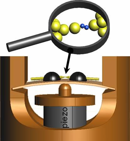
mechanically controllable break junction (MCBJ) technique, which allows a
single atom contact to be stabilized on the scale of picometers [1,2].
The behavior of atomic and molecular nanojunctions is investigated by
self-designed measurement setup. Besides the extreme stability, the MCBJ
technique also guarantees the cleanliness of the freshly broken
electrode surfaces. Molecules are deposited to the junction through a
heatable capillary tube.
Heterojunctions between electrodes with different electronic/magnetic properties are created in an STM geometry. Presently, rough actuation is performed by a mechanical transmission, and fine tuning is done by a 3D piezo actuator. A new setup where all the movements are done by piezo actuators is under construction.
When touching the studied sample with a superconducting tip, strongly nonlinear current voltage characteristics are observed, from which important information can be deduced about the polarization of the electron spin in the studied sample. This provides a unique tool to studying local nanoscale magnetic properties (Andreev spectroscopy, [3]). Besides, extreme current densities (109-1010 A/cm2) can be achieved in nanoscale junctions, by which novel ionic/magnetic switching features can be realized using appropriately chosen materials as electrodes [6,7].
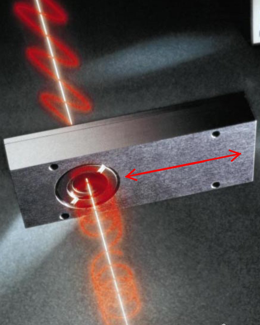 Magneto-optical spectroscopy is a fundamental tool to
obtaining information about the nature of magnetic ordering in novel
complex magnetic materials. Various fundamental parameters can be
determined like total magnetization, magnetization of some building
elements, spin-orbit interactions or the strength of exchange
interactions between spins. The principle of this method is based on the
fact that magnetic state of electrons strongly influences conduction
and optical properties. Our self-developed magneto-optical spectrometer
covers a broad interval of photon energies, and can resolve local
magnetization down to the scale of a few microns. It is used to
investigate technologically important novel materials at variable
temperature range (T=2–300K) and high magnetic fields (up to B=12T).
Theoretical description of such tiny nanocircuits is not easy, as a non-equilibrium quantum system with strong electron – electron interactions must be treated. Our theoretical group therefore applies the powerful methods of quantum field theory – also widely used in elementary particle physics. Additionally, ab initio simulations based on quantum chemistry are also employed. Special emphasis is put on the numerical renormalization group studies, which are successfully applied to the study of various nanoscale quantum systems.
Results
The short summaries below represent our recent results by highlighting some demonstrative experimental observations.
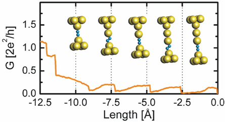 We have demonstrated that gold, well-known for its
inertness on its macroscopic surfaces, is highly reactive on the
nanoscale. According to our results, a hydrogen molecule can be
incorporated in the gold nanocontact, and this hydrogen clamp is strong enough
to pull a chain of gold atoms [8].
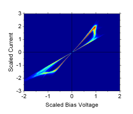
We have created a nanoscale resistive switch along the AgS ionic conductor layer between an Ag sample and a W tip. The nanojunction with diameters down to a few nanometers forms a stable, well reproducible switching device in the resistance range of a few hundred Ohms and switching threshold voltages of 0.4–0.6 V. For even smaller contact diameters, this switching mechanism is replaced by a less controlled electro-migration based switching [6, 7].
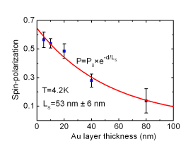 On a metal-superconductor interface, electrons are
converted to Cooper pairs through the process of Andreev reflection: the
incident electron is reflected as a hole with opposite spin, and a
Cooper pair is created in the superconductor. If we only have electrons
with a certain spin direction in the metal, then this conversion is
prohibited, as the other – opposite spin – electron of the Cooper pair
is missing. Measurement of such Andreev reflections gives valuable
information about spin ordering. Applying this technique and placing a
nonmagnetic layer between a magnetic electrode and the superconducting
tip, we can answer the question that how long a spin-memory is
preserved. The figure shows the exponential decay of spin-polarization
in an Au layer with a characteristic decay length of 53 nm.
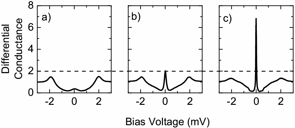
Electrons and holes taking part in the Andreev process can also form Cooper pairs in a non-superconducting material (proximity superconductivity). We can even form superconductivity in a semiconducting material through enhancing the number of phase-coherent carriers in a small region with typical thickness of 100nm. The figure demonstrates the building up of proximity superconductivity, as reflected in the growth of the zero bias coherence peak above the theoretical threshold limit of 2 [9].
In sub-micron scale circuits, electrons propagate as coherent quantum mechanical waves, exhibiting interference phenomena. At finite temperatures, however, electrons will be scattered inelastically so that their quantum mechanical phase is lost. An important source of inelastic scatterings are magnetic impurities. Our theoretical group has performed numerical renormalization group calculations to determine how magnetic impurities lead to inelastic scattering, how the strength of scattering depends on the energy of incoming electrons and on the temperature of the system. The results achieved were confirmed by later experimental studies [10].
Expected impact and further research
Research activity of the scientific workshop is related to several directions of ongoing developments in nanoelectronics. Our main goal is to achieve a detailed understanding of basic physical phenomena related to technologically highlighted topics, and the development of custom built nanostructures and novel characterization methods demonstrating novel functionalities at the nanoscale. For this purpose, we emphasize the following directions for future research:
In nanoscale circuits, electric current can be manipulated on single electron level, which enables manipulation and detection of electron spin and charge with a previously inaccessible precision. In our further research, we plan to study spin coherence in various nanostructures.
In the field of molecular electronics, we develop novel methods for the characterization of single-molecule arrangements. After contacting simple molecular gases, we plan to study conduction properties of complex organic molecules.
By the creation of nanoscale heterocontacts several interesting phenomena can be studied even at the atomic scale, well below the resolution of electron beam lithography. We plan to equip our measurement setup with inertial piezo actuators, which would enable us to perform local measurements on nanofabricated devices by creating atomic scale contacts at arbitrary positions.
The main direction of theoretical investigations is the
calculation of noise spectrum in non-equilibrium correlated systems. We
plan to improve our non-equilibrium renormalization group method, which
enables determination of spontaneous temporal fluctuations of current.
Besides, we plan a detailed study of the electron entangler device –
recently established by the experimental group – by quantum field theory
methods.
Publications, references, links
10 highlighted publications (5 from the last 5 years)
L. Hofstetter, Sz. Csonka, J. Nygard, C. Schonenberger
Cooper
pair splitter realized in a two-quantum-dot Y-junction
Nature, 461, 960
(2009).
B. Dóra and F. Simon
Electron-spin
dynamics in strongly correlated metals
Phys. Rev.
Lett. 102, 137001 (2009).
A. Halbritter, P. Makk, Sz Csonka and G. Mihály
Phys. Rev. B 77, 075402 (2008).
A. Geresdi, A. Halbritter, M. Csontos, Sz. Csonka, G. Mihály,
T. Wojtowicz, X. Liu, B. Jankó, J. K. Furdyna
Phys. Rev. B 77, 233304 (2008).
Sz.
Csonka, A. Halbritter and G. Mihály
Pulling
gold nanowires with a hydrogen clamp
Phys.
Rev. B 73, 075405 (2006).
F. Simon, H. Kuzmany, B. Náfrádi, T. Fehér, L. Forró, F. Fülöp, A. Jánossy,
L.
Korecz, A. Rockenbauer, F. Hauk and A. Hirsch
Magnetic
Fullerenes inside Single-Wall Carbon Nanotubes
Phys. Rev.
Lett. 97, 136801(2006).
Pressure induced ferromagnetism in (In,Mn)Sb dilute magnetic semiconductor
Nature Materials 4, 447 (2005).
Isotope Engineering of Carbon Nanotube Systems
Phys. Rev. Lett. 95, 017401(2005).
Sz.
Csonka, A. Halbritter, G. Mihály,
O.I.
Shklyarevskii, S. Speller, and H. van Kempen
Conductance of Pd-H
nanojunctions
Phys. Rev.
Lett. 93, 016802 (2004).
G. Zarand, L. Borda, Jan von Delft, N. Andrei
Theory of inelastic scattering from magnetic impurities
Phys. Rev. Lett. 93, 107204 (2004)
A.
Halbritter, L. Borda and A. Zawadowski
Slow
Two-Level Systems in Metallic Point Contacts
Advances in
Physics 53, 939–1010 (2004).
10 selected theses from the past 10 years (5 from the last 5 years)
Csonka Szabolcs (PhD, 2006)
Electron transport in atomic and molecular junctions
Csontos Miklós (PhD, 2007)
High pressure magnetotransport study of (III,Mn)V dilute magnetic semiconductors
Demkó László (PhD, 2010), in Hungarian
Magnetic phase diagram of correlated d-electron systems
Geresdi Attila (MSc, 2007), in Hungarian
Spin-polarization of charge carriers in magnetic semiconductors
Gyenis
András (MSc, 2010), in Hungarian
Resistive memory effects in atomic and
mesoscopic contacts
Halbritter András (PhD, 2003)
Investigation of atomic-sized conductors with the mechanically controllable break junction technique
Kézsmárki István (PhD, 2003)
Phase diagram of a correlated d-electron system: experimental study of BaVS3
Dóra Balázs (PhD, 2002)
Simon Ferenc (PhD, 2002), in Hungarian
Analysing strongly
correlated electron systems by magnetic resonance method
Zaránd Gergely (PhD, 1995)
Renormalization group study of the low temperature behavior
of two level systems
Participants:
|
|
|
|
|
|
||||
|
|
||||||||
|
|
|
|
|
|
|
|
|
|
