 |
BMe Research Grant |

|

Doctoral School of Electrical Engineering
Department of Electronic Technology
Supervisor: Gábor Harsányi, DSc
Investigation of micro- and nanostructures with atomic force microscopy and electrochemical methods
A short introduction to the field of research
The investigation of surface or bulk micro- and nanostructures is one of the most interesting and widespread fields of applied research nowadays. Through the examination of material structures we can gain understanding about their conformation that can be used to improve their properties in a large variety of application fields. The advanced investigation methods of our times – such as atomic force microscopy, which grants us nearly atomic scale resolution – enable new aspects of examination on material systems, but there is always a need for new and innovative methods of investigation as well.
A short introduction to the research facility
The Sensors and Microfluidics Laboratory under Dr. Hunor Sántha is established in the applied research and development of biomedical sensors, biosensors and microfluidic devices. The laboratory has been successfully involved in several national and international projects in recent years, and its budget spent on research and development over the last 4 years exceeds 460 million Forints. In 2012, our team won the ”Best Innovation of 2011” award of the Pro Progressio Foundation.
An introduction to the background of the field of research
The general aim of my work is to demonstrate that through combined application of state of the art investigation methods from different research fields (disciplines) we can design such novel investigation methods that allows us to solve problems which could not be solved earlier by applying methods from any single discipline; or to gain a more detailed insight into the examined system. In my work, I combined methods from the field of electrochemistry (e.g. amperometry, voltammetry, electrochemical impedance spectroscopy (EIS)) with state of the art micro/nano examination methods from the field of materials science and technology (e.g. atomic force microscopy (AFM), scanning electron microscopy (SEM), and electron backscattered diffraction (EBSD)) for the investigation of three different material systems: 1) structural investigation of the surface structure of gold thin films; 2) investigation of ferrite grain orientation of cast iron; 3) investigation of lead-free solder microstructures.
1) Gold thin films are often utilized as transducer elements in chemical, electrochemical or optical sensors due to their several technologically favorable properties. The structure of the polycrystalline gold thin films – which can be easily manufactured with vacuum technologies – largely depends on the technological parameters of the process and the applied substrate, so the quality of the gold thin films available on the market varies significantly, which could affect their possible application (Figure 1). In the case of electrochemical measurements for example, the quality of the gold thin films is an important parameter to perform precise measurements with electrodes fabricated from the thin films. In EIS measurements, the gold thin film electrodes show a behavior called “capacitance dispersion”, which makes the precise determination of the electrode capacitance more difficult and which phenomenon depends on the surface quality of the thin film. There is a debate in the literature about the possible causes of this capacitance dispersion, and whether the surface structure or the surface roughness of the electrodes could be related to it and to what extent [1].
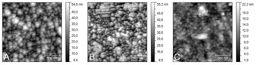
Fig. 1: Contact AFM images of technologically different gold thin films.
2-3) Sample pretreatment is a key step in the microscopic investigation of metallic materials. To reveal the microstructure of the samples they often utilize different kinds of chemical treatments (e.g. etching) besides the standard mechanical polishing. Generally, it can be said about the currently applied sample pretreatment methods that the revelation of the three dimensional microstructures is limited in detail, and that the precise working mechanism behind some of the applied methods are often not fully understood.
Aim of the research, questions to be answered
1) It can be stated that there exist no precise method for the determination of the surface roughness, surface structure or effective electrode surface area due to the imperfection of the electrochemical and microscopy methods [2]. Although AFM is frequently used for the detailed characterization of surface topography, the most widely used surface roughness parameters (e.g. Ra and RRMS) are simple average based values which do not consider the spectral distribution of the measured height points (the shape of the surface structures). So it can possibly happen that we obtain the same surface roughness value for two structurally very different surfaces. Hence my aim is to introduce and analyze a completely new parameter for the quantitative structural characterization of surfaces measured with scanning probe microscopy, which takes into account the spectral distribution of the measured height points (zi), in other words the shape and localization of the surface structures. Also, my other goal is to investigate the possible correlation between this new parameter and the capacitive behavior of the electrodes fabricated from the characterized thin films, in contrast to the surface roughness parameters.
2) It is widely known in the literature that the etching speed of the chemical and color etching methods used for the pretreatment of cast iron depends on the crystallographic orientation of the ferrite grains [3]. My first aim with this investigation is to determine the precise working mechanism behind these treatment methods and then to develop a novel method which would enable the determination of the crystallographic orientation of the ferrite grains by applying solely color etching and optical microscopy, without the need for using more expensive methods and equipment (such as EBSD).
3) The standard sample pretreatment methods applied for the investigation of solder joint microstructures enable the examination of microstructures in a two dimensional perspective, but the revelation of the three dimensional structures is limited in detail. My aim in this field is to apply electrochemical methods to improve the pretreatment of samples.
Methods
The methods of investigation cover electrochemical, optical microscopy, atomic force microscopy and scanning electron microscopy techniques. Atomic force microscopy (AFM) is a member of the scanning probe microscopy (SPM) family with one of the highest resolution. I utilized contact and tapping modes for the structural investigation of gold thin films and for the determination of ferrite grain height after etching. Besides the classical optical microscopy, scanning electron microscopy (SEM) is also a widely established investigation method in metallurgy. Along with SEM imaging energy dispersive spectroscopy (EDS) could be used for the determination of material compositions (e.g. identification of the intermetallic compounds in solder joints), while electron backscattered diffraction (EBSD) can be utilized for the determination of the crystallographic orientation of metallic grains.
For the investigation of metallic materials with various microscopy methods I applied several different sample pretreatments. After the standard mechanical polishing, cast iron samples were either chemically etched in 2 % nital or color etched with the Beraha-1 type solution. In the latter case an interference layer composed mostly of sulfates builds up on the ferrite grains and due to the crystal orientation dependent etching speed the thickness of the interference layer will vary along the different grains. In a given layer thickness range this phenomenon colors the grains differently (Fig. 2).
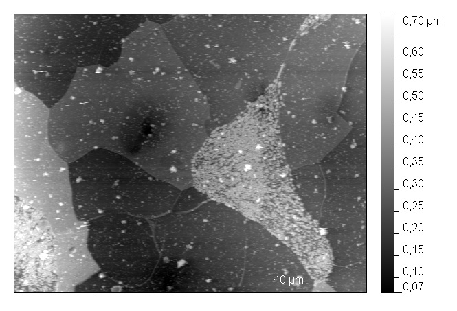
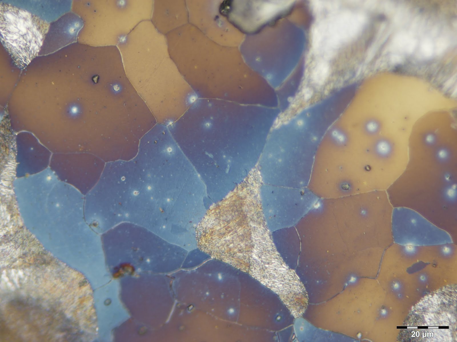
Fig. 2: Left: AFM image of a cast iron specimen etched with 2 % nital; Right: optical microscope image of the same specimen after color etching
During my work I applied electrochemical methods both for sample pretreatment and for sample characterization (measurements) as well. For the investigation of the capacitive behavior of gold thin film electrodes I utilized electrochemical impedance spectroscopy (EIS). For the investigation of solder joint microstructures I developed an own method based on amperometry. The principle of the method is that in mild sulfuric acid it is possible to selectively remove the bare tin phase from the solder joint – without any harm to the intermetallic microstructures – in a controlled way utilizing the different reduction potentials of the thin and intermetallic phases. This method is both a sample pretreatment and a characterization technique at the same time, because the measurement of amperometric current allows us to determine the amount of removed tin phase, and with this to quantitatively characterize the solder joints.
Results
1) I introduced a new parameter called localization factor which carries information about the surface structure and can be used for the quantitative characterization of the surfaces with AFM. The localization factor can be determined by calculating the generalized localization of an AFM image, which can be derived from the structural entropy and the spatial filling factor functions of the image. The localization factor is the value (��) which yields the smallest square error between the generalized localization of the image and the generalized localization of the exp(-x(��)) probe function. I demonstrated with measurements that this new parameter can be used to identically characterize gold thin film surfaces with contact mode AFM in the 1-900 um2 scan range. Compared to the surface roughness parameters, the localization factor gives supplementary information about the characterized surfaces because it takes into account the shape and localization of the surface structures. I proved with AFM and EBSD measurements that after thermal annealing on 300 oC for 5 minutes the grain structure of the gold thin films changes in a way, that there is no significant difference in the measured surface roughness before and after the annealing, regardless of the visually obvious structural change. Based on these results I pointed out that the previously experienced change in the capacitance dispersion of the gold thin film electrodes after the annealing [1] could possibly originate from the structural transformation of the grain structure, without measurable change in the surface roughness. I proved that the localization factor is capable of the quantitative characterization of the change in the gold surface structure caused by thermal annealing.
2) I investigated the working mechanisms of chemical and color etching as cast iron pretreatment methods with AFM and EBSD. I found out that the 2% nital chemical etchant etches the ferrite grains in a crystal orientation dependent way, and that the etching speed and the gradient of the etching speed along a given grain both correlate with the angle between the specimen normal and the [001] direction. The higher the angle between the grain normal and the [001] direction the higher the etching speed is and a smaller the gradient of the etching speed along that grain. I found that the Beraha-1 solution which is used for color etching forms an interference layer on top of the ferrite grains which – contrary to previous theories [3] – does not have uniformly smooth surface. The etching speed of the Beraha-1 solution is also depending on the grain orientation and it is just the opposite as in the case of nital etching. The higher the angle between the grain normal and the [001] direction the smaller the speed of the interference layer formation will be. I also found that over etching the surface with the Beraha-1 solution causes streaks on the surface of machined cast iron specimens (Fig. 3.). The direction of the streaks depends on the angle between the grain normal and the [001] direction; this phenomenon together with color etching could be used to deduce the orientation of grains with the help of only an optical microscope. (Note: these findings are the result of the cooperation with Dr. Péter J. Szabó from the Department of Materials Science and Engineering, BUTE.)
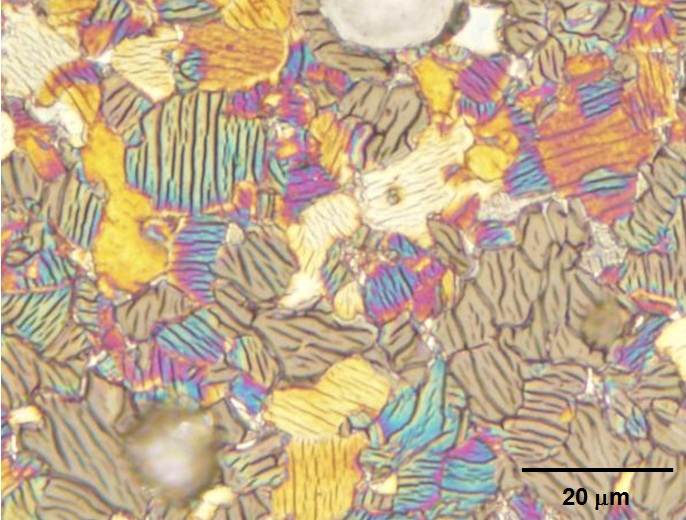
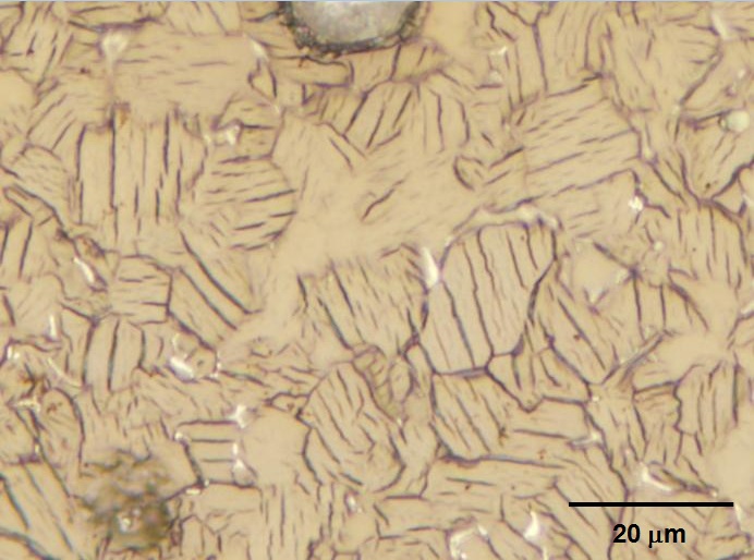
Fig. 3.: Optical microscopy images presenting the streaking of the ferrite grains after color etching
3) I designed an electrochemical method to selectively remove the bare tin phase from lead-free solder joint samples. This new method not only reveals the solder microstructures in a detail unknown to any other methods previously available (Fig. 4.), this novel technique also enables the quantification of the removed tin from the solder joint. In this way, the bare tin / intermetallic compound ratio of the solders can be determined which could be a very valuable asset in this field of research. Note: the development of this novel method is the joint merit of Mr. Tamás Hurtony, a fellow PhD student at our department and me. We are currently working on the application of the method for the structural comparison of different solder microstructures with their mechanical and reliability properties.
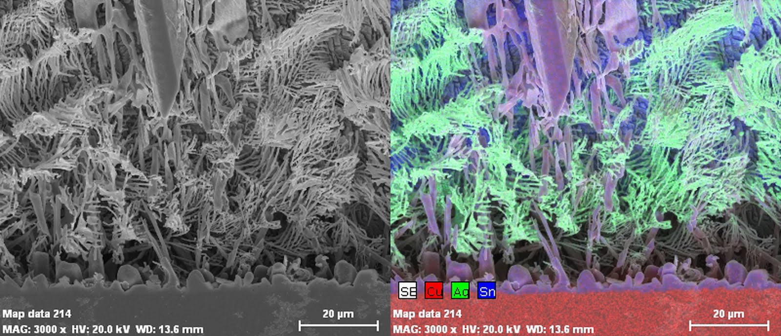
Fig. 4: SEM (left) and SEM-EDS (right) images of the intermetallic solder microstructures after the selective removal of the bare tin phase
Expected impact, further research
The application of localization factor the new parameter I introduced goes beyonds the characterization of gold thin films. This parameter could also be applied in any field, where surface structure plays a role in the investigated phenomenon, and presumably it could be used most effectively in conjunction with the other surface roughness parameters to obtain a more comprehensive picture about the characterized surfaces. In the field of gold thin film investigations we plan to reproduce the electrochemical measurements with the help of Dr. Tamás Pajkossy in the Chemical Research Center this autumn.
Our new electrochemical pretreatment method receives significant scientific interest: e.g. at the 35th International Spring Seminar on Electronics Technology conference I received “Best Oral Presentation” award for my presentation in this topic. As a following up Prof. Klaus-Jurgen Wolter, an international expert in this field invited us to the University of Dresden to discuss a possible future cooperation based on this method with his team. Our method also raised some industrial interest as well from the “Robert Bosch Elektronika Kft.” During the summer we would also like to start the patenting process of our novel method with Mr. Tamás Hurtony.
Parts of my results were applied in the four European Union FP-6 projects in which our department participated (“DINAMICS”, “DVT-IMP”, “RaSP” and “u-Builder”). I also participated with my results in the BUTE Research University NNA P4-T3 and P2-T1 projects.
Publications, references, links
A. Bonyár, L. M. Molnár, G. Harsányi, ”Localization factor: a new parameter for the quantitative characterization of surface structure with atomic force microscopy (AFM)”, MICRON, 43, (2012) pp. 305-310.
A. Bonyár, P. J. Szabó, ”Correlation between the grain orientation dependence of color etching and chemical etching”, MICROSCOPY AND MICROANALYSIS – accepted, in press
P. J. Szabó, A. Bonyár, ”Effect of grain orientation on chemical etching”, MICRON, 43, (2012), pp. 349-351.
T. Hurtony, A. Bonyár, P.Gordon, G Harsányi ”Investigation of intermetallic compounds (IMC) in electrochemically stripped solder joints with SEM”, MICROELECTRONICS RELIABILITY, 52, (2012), pp. 1138-1142.
A. Bonyár, L. M. Molnár, G. Harsányi, “Dependence of the surface roughness and localization factor parameters on the background correction of AFM images: a thin film characterization study”, MATERIALS SCIENCE FORUM – accepted, in press
T. Hurtony, A. Bonyár, E. Harkai, P. Gordon “Microstructure comparison of soldered joints using electrochemical selective etching”, MATERIALS SCIENCE FORUM – accepted, in press
A. Bonyár, H. Sántha, B. Ring, M. Varga, J. G. Kovács, G. Harsányi ”3D Rapid Prototyping Technology (RPT) as a powerful tool in microfluidic development” PROCEDIA ENGINEERING 5, (2010), pp. 291-294.
A. Bonyár, I. Bosznai, H. Sántha and G. Harsányi, ”A custom-developed, handheld EIS measurement platform”, IFMBE PROCEEDINGS, Vol. 37. 2011 (Springer)
A. Bonyár, H. Sántha, B. Ring, and G. Harsányi, ”A custom-developed SPRi instrument for biosensor research”, IFMBE PROCEEDINGS, Vol. 37. 2011 (Springer)
H. Sántha, A. Bonyár, ”Modular Biosensor Reaction-Cell.” PERIODICA POLYTECHNICA-ELECTRICAL ENGINEERING 52:(1-2), (2008), pp. 95-109.
Bonyár Attila, "Az atomerő mikroszkópia (AFM) alkalmazása a bioérzékelő- kutatásban. (in Hungarian) ELEKTRONET XX.:(3) pp. 38-39. (2011)
Bonyár Attila, Sántha Hunor, Varga Máté, Ring Balázs, Harsányi Gábor "A 3D RPT (Rapid Prototyping Technology) alkalmazása mikrofluidikai eszközök fejlesztéséhez.” (in Hungarian) LABORATÓRIUMI INFORMÁCIÓS MAGAZIN 6: pp. 10-12. (2010)
A. Bonyár, G. Harsányi, ”CPE investigation of gold thin films”, Proc. of the 17th International Symposium for Design and Technology of Electronics Packages. Timisoara, Romania, 2011 (IEEE)
A. Bonyár, G. Harsányi, ”Typical Problems and Solutions in Electrochemical Measurement Cell Development.” In: Proc of the 33rd International Spring Seminar on Electronics Technology, Warsaw, Poland, 2010 (IEEE)
A. Bonyár, T. Hurtony, G. Harsányi, ”Selective electrochemical etching for the investigation of solder joint microstructures”, Proc of the 35rd International Spring Seminar on Electronics Technology. Bad Ausse, Austria, 2012 (IEEE)
A. Bonyár, G. Harsányi ”AFM nanoshaving: a novel prospect for the structural comparison of bioreceptor layers.” In: Proc of the 34th International Spring Seminar on Electronics Technology. Tatranska Lomnica, Slovakia, 2011 (IEEE)
A. Bonyár, H. Sántha, ”Novel Interdigitated Transducer Structures for Biosensoric Applications.” In: Proc of the 32nd International Spring Seminar on Electronics Technology. Brno, Czeh Republic, 2009 (IEEE)
A. Bonyár, H. Sántha, ”Electrochemical characterization of DNA covered gold thin film electrodes for biosensoric applications.” In: Proc. of the 31st International Spring Seminar on Electronics Technology, Budapest, Hungary, 2008 (IEEE)
H. Sántha, B. Ring, K. Szalay, A. Bonyár, ”A custom-built surface plasmon resonanace (SPR) imaging device for biosensor applications”, Euronanoforum 2011, Budapest
A. Bonyár, H. Sántha, ”Comparison of electrode setups for a custom built electrochemical measurement platform for DNA based biosensors”, In: 1st Bio-sensing Technology Conference. Bristol, United Kingdom, 2009
[1] Tamás Pajkossy, ”Impedance spectroscopy at interfaces of metals and aqueous solutions – surface roughness, CPE and related issues”, Solid State Ionics 176 (2005) 1997-2003.
[2] S. Trasatti, O. A. Petrii, "Real surface area measurements in electrochemistry", Pure & Appl. Chem., Vol 63, No. 5, 1991, pp. 711-734.
[3] P. J. Szabó, I. Kardos "Correlation between grain orientation and the shade of color etching”, Materials Characterization 61 (2010) 814-817
Sensors and Microfluidics Laboratory Homepage
Nanotechnology Laboratory Homepage
BUTE Research University NNA P4-T3 Project Homepage
BUTE Research University NNA P2-T1 Project Homepage