 |
BMe Research Grant |

|

Doctoral School of Physics
Department of Atomic Physics
Supervisor: Dr. Adam Gali
Semiconductor Nanocrystals for Biomarker and Solar Cell Applications
Introducing the research area
My research is devoted to the investigation of the optical properties of nanometer sized group four semiconductor crystals (nanocrystals, also known as quantum dots) for in vivo bioimaging and solar cell purposes. My work is mostly theoretical, I simulate the optical properties of nanocrystals using first principles theories.
Brief introduction of the research place
My PhD work has been carried out as a member of the group of Prof. Adam Gali at the Department of Atomic Physics, Budapest University of Technology and Economics. We used our local computer cluster for small test calculations; large production runs required using the supercomputers of international collaborations, grants.
History and context of the research
Thanks to the ever improving experimental techniques, producing and working with nanocrystals can be done routinely in the laboratories nowadays. In some special cases, controlling the position of every single atom is also possible.
These nanocrystals may have special physical properties due to their small size. E.g. contrary to non-luminescent millimeter sized crystallites, nanocrystals may have measurable luminescence. Furthermore, the color of such nanocrystals can be tuned by their size, which is an interesting property all by itself. Both these effects can be attributed to a quantum mechanical phenomenon, commonly referred to as ’quantum confinement’.
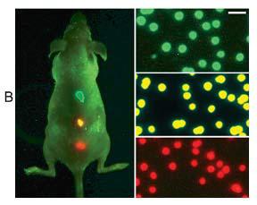
Sensitivity and multicolor capability of nanocrystal imaging in live animals. Left: a mouse with nanocrystal labeled organs. Right: nanocrystal labeled microbeads emitting green, yellow or red light depending on the size of the nanocrystal [1].
Since in the nanometer size regime, the surface/volume ratio changes considerably with respect to the bulk case, the surface bears special importance. Its presence can change the physical properties of the system, completely overriding/hiding quantum confinement induced effects. On the one hand, this is a drawback, since one has to be extremely cautious when it comes to making nanocrystals, on the other hand this unique property gives the researchers a new knob to turn: by changing the ligands at the surface or by manipulating surface atoms one may easily tune the properties of nanocrystals towards the desired direction.
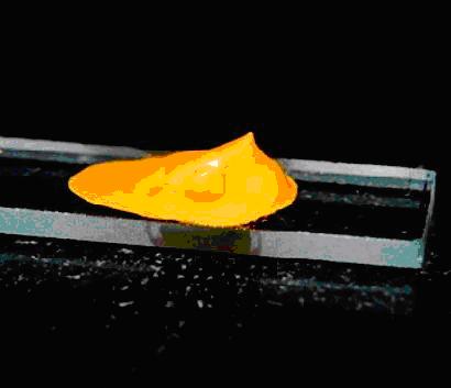
Paintable solar cell made out of cadmium sulfide (CdS) nanocrystals [2]. The color of the paint can be tuned by the size of the nanocrystals.
Several research groups realized that by using the small size and size-tunable color of nanocrystals, it could be possible to achieve bioimaging of human cells [1]. The size-tunable color could be an advantage too when it comes to solar cells: if one can cover the full solar spectrum by nanocrystals of different sizes, absorbing most of the incoming light, one may build a more effective solar cell [2,3].
The research goal, open questions
The main goal of my research, which I call computational materials science, is twofold. First, I believe that I can help experimentalists by looking at details in the simulations which are hard to access in the experiments. Second, as the accuracy and predictive power of computations are improving, it is more and more important to not only understand already existing experiments, but to predict new functionalities. This is actually very important, because carrying out experiments is usually much more expensive than doing the same experiment on computers.
So far I have been dealing with group four semiconductor nanocrystals. Accordingly, my work can be partitioned into two major areas following the rows of periodic table: diamond and silicon nanocrystals.
Diamond nanocrystals
According to a recent paper, 99% pure diamond nanocrystal samples can be produced [4]. This is a real experimental breakthrough, because the atomic structure of these diamondoids is known, thus they are ideal testbeds for experiments and theories as well. Since we had access to high precision experimental data regarding the optical properties of these diamondoids [4], I decided to examine them by computations.
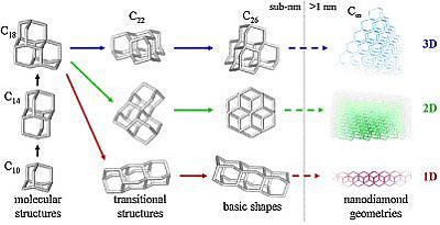
Structures of the smallest diamond nanocrystals, also known as diamondoids: gray tubes represent covalent bonds between neighbor carbon atoms. Note that similarly to bulk diamond, carbon atoms have tetrahedral coordination, thus similar physical properties are expected. The smallest diamondoid, adamantane is shown in the lower left corner (labeled by C10).
Silicon nanocrystals
Arthur Nozik, a fellow of the American NREL Institute is in the forefront of the research of third generation solar cells [5,6]. A paper published by Nozik in 2002 [7] grabbed considerable interest from the scientific community as it was the first paper to suggest that nanocrystal solar cells may be the first representatives of efficient and cheap third generation solar cells. This is due to an effect called Multiple Exciton Generation (MEG). The promise of MEG is that more than one electron-hole pair could be extracted at a price of one absorbed photon, thus the overall efficiency of the solar cell is enhanced. As part of my work I looked at the MEG effect in silicon nanocrystals, as silicon is the most important material so far in the solar industry [8].
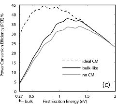
Theoretical maximum efficiency of solar cells exploiting the MEG effect (here MEG is referred to as CM, Carrier Multiplication) [9]. Ideal MEG solar cells may reach 44% efficiency, as a comparison the best theoretical efficiency of single junction silicon solar cells is ~32% [5].
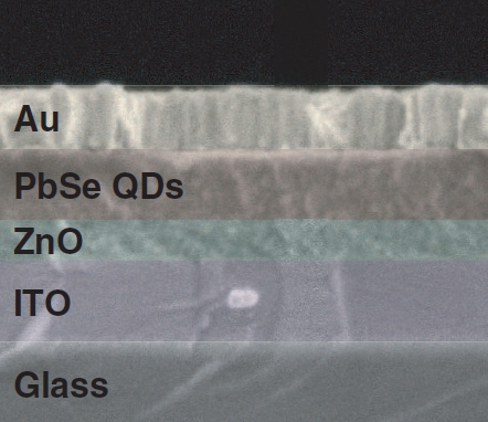
False color cross sectional view of the first lead-selenide (PbSe) nanocrystal solar cell, where the MEG effect was proved to exist. The overall efficiency of the device was over 4% [10].
Methodology
Modeling at the atomic level
In the nanometer size regime the quantum mechanical nature of electrons cannot be neglected, thus the Schrödinger equation in its full realm needs to be addressed. Unfortunately, the exact solution of the equation is only solvable for few electron systems. Systems containing more electrons need special treatment. Density functional theory (DFT) is an in principle exact way to deal with the many electron problem. In practice, several approximations are made to make the equations feasible. In this approach, electrons move in a mean field, thus in essence DFT is a mean field theory. Usual DFT calculations give the properties of the system without any external field, in order to deal with that, its extension, time-dependent density functional theory (TDDFT) needs to be used, which is capable of calculating the optical properties of the system of interest. In case of the silicon nanocrystals I derived equations based on perturbation theory to deal with the MEG relaxation mechanism of electron-hole pairs. These equations have been implemented in an open-source DFT code.
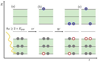
The process of MEG. (a) If a photon with energy of two times larger than the band gap is absorbed (b) then the generated hot carriers may decay to (c) biexcitons by exciting an additional electron-hole pair via inelastic Coulomb scattering. Interactions which mediate the processes are also depicted: dipole (er) for the absorption process and screened Coulomb interaction (W) for impact ionization.
Supercomputers
These calculations are still very computationally intensive. The scaling is N3 (N4) for DFT (TDDFT), where N is the characteristic size of the system. This scaling means that if one doubles the size of the system than the time needed to calculate the same property is eight (sixteen) times more. This behavior requires the usage of efficient computational techniques. Basically, there are two different ways to enhance the efficiency of such computations: either the specific algorithm to integrate the equations is improved, or the program is changed to utilize more than one computing unit (processor) at the same time. We concentrated on the second approach: our largest simulations use 128-256 processors and typical wall-clock times (this is the time measured from the start to the completion of a calculation) range from days to weeks.

Supercomputer at the Wigner Research Centre for Physics, several nodes can be found in a rack, the smallest module, an infiniband switch is responsible for the fast connection between nodes.
Results
Diamond nanocrystals
I showed that optical absorption spectra calculated by TDDFT calculations are in good agreement with the experiments. These calculations also showed that Rydberg excitations govern the low energy part of the optical spectrum even for larger diamondoids [V1,V2]. These low energy Rydberg states are very well known for organic molecules and as far as I know this was the first time that their existence was proposed for large nanocrystals. This unexpected finding may explain the good electron emitting property of diamondoid covered gold surfaces [11].
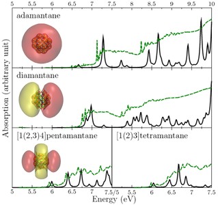
The experimental (green dashed line) and theoretical (black continuous line) absorption spectrum of several diamondoids [V1,V2]. Inset: red-yellow blobs represent s, p, d Rydberg states, respectively.
I also investigated the possibility of modifying the optical properties of diamondoids by putting specific ligands on the surface. I found that double bonded sulfur atoms push the optical gap towards the visible/infrared range [V2,V3]. This finding, together with the biocompatibility of diamond, may help in realizing a new generation of in vivo biological markers.
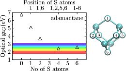
Left: the optical gap of the smallest diamondoid, adamantane, as a function of sulfur-carbon double bonds at its surface. The more sulfur atoms are on the surface, the smaller the gap will be: in the case of 4,6 sulfur atoms the optical gap reaches the desired visible region of the electromagnetic spectrum [V3]. Right: the ball-and-stick structure of adamantane, cyan balls depict carbon atoms. The numbers on the atoms represent carbon atoms to which sulfur atoms bond.
Silicon nanocrystals
I showed that the optical absorption of silicon nanocrystals strongly depends on its surface structure, and possible surfactants. This finding explained several contradictions in the experimental reports: sample-to-sample variations may drastically change the optical properties of the system [V4]. Following this path, I developed a code based on density functional theory and perturbation theory, which is capable of calculating the MEG rate for nanocrystals in the most accepted impact ionization picture. I found that surface reconstructions enhanced the impact ionization rate [V5]. This message translates to enhanced solar conversion efficiency, which is the ultimate goal of the solar cell research. Motivated by these finding,s we have also looked at silicon nanocrystals made out of high pressure phases of silicon: our results showed that these nanocrystals can be even more promising due to their lower optical gap [V6].
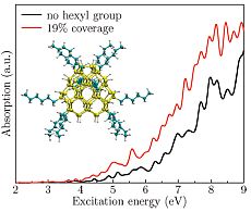
The enhancement in the absorption of silicon nanocrystals as an effect of hexyl group coverage [V4].
Expected impact and further research
My publications received 22 independent citations up to date. My publication regarding the absorption of silicon nanocrystals was featured in MRS Bulletin, and it is cited by the most recent Nature paper [11]. I presented my results on several international conferences and my poster presented at the workshop "Time-dependent density Functional Theory: prospects and applications” was selected as one of the best posters. Furthermore, I recently won the possibility to organize next year’s European Theoretical Spectroscopy Facility (ETSF) Young Researchers’ Meeting, which is an annually held workshop for young scientists working in the field of theoretical spectroscopy.
The physics of nanocrystals is broad enough to have many possible research directions. E.g. it is also interesting to look at some specific atomic defects in semiconductors, the so called color centers. Their name comes from the fact that, not surprisingly, they change the color of the host crystal. Interestingly, some of these defects may be the forerunner of solid state quantum computers [12]. The existence of such defects in nanocrystals has been recently reported [13].
Publications, references, links
Publications
[V1] Márton Vörös and Adam Gali, Optical absorption of diamond nanocrystals from ab initio density functional calculations
Physical Review B 80, 161411(R) (2009)
[V2] Márton Vörös, Tamás Demjén, Adam Gali, The Absorption of Diamondoids from Time-dependent Density Functional Calculations
MRS Spring Meeting Proceedings 1370, mrss11-1370-yy02-07 (2011)
[V3] Márton Vörös, Tamás Demjén, Tibor Szilvási, Adam Gali, Tuning the optical gap of nanometer-size diamond cages by sulfurization: A time-dependent density functional study
Physical Review Letters, accepted (2012)
[V4] Adam Gali, Márton Vörös, Dario Rocca, Gergely T. Zimanyi and Giulia
Galli, High Energy Excitations in Silicon Nanoparticles
[V5] Márton Vörös, Dario Rocca, Giulia Galli, Gergely T. Zimanyi and Adam Gali, Increasing the efficiency of Multiple Exciton Generation in Si nanoparticles: an ab-initio study
Physical Review Letters, under review
[V6] Stefan Wippermann, Márton Vörös, Dario Rocca, A. Gali, G. T. Zimanyi and G. Galli, High pressure phase Si nanoparticles: Applications to solar energy conversion
In preparation
Other publications
[V7] Márton Vörös, Péter Deák, Thomas Frauenheim, Adam Gali, The absorption spectrum of hydrogenated silicon carbide nanocrystals from ab initio calculations
Applied Physics Letters 96, 051909 (2010)
[V8] Márton Vörös, Péter Deák, Thomas Frauenheim, Adam Gali, The absorption of oxygenated silicon carbide nanoparticles
The Journal of Chemical Physics 133, 064705 (2010)
[V9] Márton Vörös, Péter Deák, Thomas Frauenheim, Adam Gali, Time-dependent density functional calculations on hydrogenated silicon carbide nanocrystals
Mater. Sci. Forum 679 - 680, 516 (2011)
[V10] Márton Vörös, Péter Deák, Thomas Frauenheim, Adam Gali, Influence of oxygen on the absorption of silicon carbide nanoparticles
Mater. Sci. Forum 679 - 680, 520 (2011)
[V11] Márton Vörös, Adam Gali, Efthimios Kaxiras, Thomas Frauenheim,
Jan Knaup, Identification of defects at the interface between 3C-SiC quantum dots and a SiO2 embedding matrix
Phys. Status Solidi B 249, 360 (2012)
[V12] Jan Knaup, Márton Vörös, Péter Deák, Adam Gali, Thomas Frauenheim,
Efthimios Kaxiras, Annealing Simulations to Determine the Matrix Interface Structure of SiC Quantum Dots Embedded in SiO2
Phys. Status Solidi C 7, 407 (2010)
Links
The group of Adam Gali:
Wikipedia articles:
http://en.wikipedia.org/wiki/Multiple_exciton_generation
http://en.wikipedia.org/wiki/Nanocrystal
UC Davis:
http://physics.ucdavis.edu/zimanyi/
NREL:
References
[1] Maureen A Walling, Jennifer A Novak, and Jason R. E Shepard, Quantum Dots for Live Cell and In Vivo Imaging
[2] Matthew P. Genovese, Ian V. Lightcap, and Prashant V. Kamat, Sun-Believable Solar Paint. A Transformative One-Step Approach for Designing Nanocrystalline Solar Cells
[3] Illan J. Kramer and Edward H. Sargent, Colloidal Quantum Dot Photovoltaics: A Path Forward
[4] L. Landt, K. Klunder, J. E. Dahl, R. M. K. Carlson, T. Moller, and C. Bostedt, Optical Response of Diamond Nanocrystals as a Function of Particle Size, Shape, and Symmetry
Phys. Rev. Lett. 103, 047402 (2009)
[5] W. Shockley and H. J. Queisser, Detailed Balance Limit of Efficiency of p-n Junction Solar Cells
Journal of Applied Physics 32, 510 (1961)
[6] M. Green, Third generation photovoltaics: advanced solar energy conversion,
Springer series in photonics, Springer, 2006
[7] A. J. Nozik, Quantum Dot Solar Cells
Physica E: Low-dimensional Systems and Nanostructures 14, 115 (2002).
[8] Trinh, M. T., Limpens, R., de Boer, W. D. A. M., Schins, J. M., Siebbeles, L. D. A., and Gregorkiewicz, T., Direct generation of multiple excitons in adjacent silicon nanocrystals revealed by induced absorption
Nature Photonics 6, 316 (2012)
[9] Gautham Nair, Liang-Yi Chang, Scott M. Geyer, and Moungi G. Bawendi, Perspective on the Prospects of a Carrier Multiplication Nanocrystal Solar Cell
[10] Octavi E. Semonin, Joseph M. Luther, Sukgeun Choi, Hsiang-Yu Chen, Jianbo Gao, Arthur J. Nozik, Matthew C. Beard, Peak External Photocurrent Quantum Efficiency Exceeding 100% via MEG in a Quantum Dot Solar Cell
[11] L. Yang et al., Monochromatic Electron Photoemission from Diamondoid Monolayers
[12] L. Childress et al., Coherent Dynamics of Coupled Electron and Nuclear Spin Qubits in Diamond
[13] Yi-Ren Chang et al., Mass production and dynamic imaging of fluorescent nanodiamonds
Nature Nanotechnology 3, 284 (2008)