 |
BMe Research Grant |

|

Doctoral School of Electrical Engineering
Department of Electronics Technology
Supervisor: Dr. Gordon Péter, associate professor
Characterization of the intermetallic compounds of lead-free solder alloys
Short overview of the research field
Reviewing the scientific literature of lead-free solder alloys and soldering techniques, we can conclude that no standardized and universal observation method exists for the characterization of the fine microstructures created by new physical processes applied in the emerging lead-free solder alloy technologies.
The goal of my research is to develop new observation methods capable of answering the new questions raised by the industry.
Introduction of the research facility
The Department of Electronics Technology was established in 1964 to teach and research the different fields of materials science, physical design and technology directly applicable in electronics industry. The Department makes emphasis on establishing partnerships with the industry in supplying skillful engineers, organizing postgraduate courses and training, carrying out research and development projects; and providing solutions to various topics in microelectronics and technology.
Preliminaries of the research
Nowadays, majority of solder joints are prepared by reflow soldering technique, where Sn in the molten solder, wetting the soldering surfaces chemically reacts with the substrate. As a result, a continuous layer of Cu-Sn intermetallic compound (IMC) is formed. The thickness of this layer is getting bigger pretty fast during the soldering and the growth won’t stop after the solidification. [1].
The mechanical properties of the solder joint are determined by the microstructure, especially by the thickness and the characteristics of the intermetallic layer (IML) between the substrate and the solder alloy. (Fig. 1.) [2].
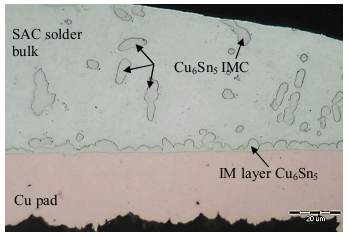
Fig. 1. Cross-section of reflowed SAC solder alloy on copper pad of FR4 substrate after Oxide-Polishing. Optical microscope image.
Nowadays, electronic industry mainly uses lead-free solder alloy (e.g. Sn-Ag-Cu, SAC) for the manufacture of electronics assemblies. With the introduction of lead-free soldering elevated technological temperature and the use of binary or ternary solder alloys have led to the emergence of new phenomenons [3‑4].
IMCs fractions spalling off the IML during the soldering process get into to the solder bulk and change its original properties. Therefore, the mechanism of spalling is a reliability issue. (Fig. 1.) [5].
The aim of the research, questions to be answered
Since the typical size of soldering specimens are much more smaller than the size of the oven, the experimental verification of the kinematic model of the solder microstructure formation cannot be performed with convectional reflow technique. Therefore, more precise validation of previously developed models require a selective and reproducible new heat transferring method.
The most commonly used metallographic test method is cross-sectioning combined with microscopy and/or scanning electron microscopy.
The general indicator of the presence of a solder connection is the existence of an IML and its proper quality. Therefore, majority of test methods focus on the determination of the average thickness of the IML. It is conceivable, however, that average thickness alone cannot fully characterize the solder, because of significant impact of the IML structure. [6]. This is the reason why I had to develop a new method for characterizing the IML.
The biggest disadvantage of cross-sectioning is the relatively narrow slice of the microstructure it can characterize, and allow very limited insight into the intermetallic structure in the solder joint. This is why we developed an electrochemically enhanced etching method, which reveals the intermetallic microstructures in the cross-sectional solder joint samples in unparalleled detail.
.
Methods
For the preparation of reproducible solder joint I set out of the selective laser soldering method. During laser soldering the energy for the reflow of the solder paste is transferred locally by the means of irradiation. The big advantage of laser soldering is that the parameters of the laser can be controlled precisely. The small scales and the big temperature differences induced by the laser makes the direct temperature measurement impossible, therefore I had to develop a physical model and a simulation program for determining the temperature profile.
For the verification of the model cylindrical symmetric experimental setup is used. By optically detecting the melting event of solder alloy I can determine the single fitting parameter of the simulation.
Cross-sectional samples are prepared from the laser soldered joints. I optimized sample preparation parameters so that the highest contrasts can be achieved during optical observation between the IMC and the solder material.
For the evaluation of optical micrographs I develop an image processing algorithm. Evaluated data will be correlated with soldering parameters as well as with the macroscopic mechanical properties (micro hardness shear force, etc) and technological parameters.
To explore the microstructure a selective electrochemical etching is developed.
Results
I have developed a physical model to describe the process of laser heat treatment. Based on this model a simulation program has been developed, which takes the material transport – such as the heat transfer – into account and which calculates the heat profile.
In the model a frequency tripled Nd:YAG laser is used in pulsed mode for coupling the energy into the cylindrical symmetric experimental setup. The model deals with the real intensity profile of the laser and the fluctuation of the reflection coefficient. The simulation solves the differential equation of the heat and material transfer for determining the heat profile and distribution. (Fig. 2.)
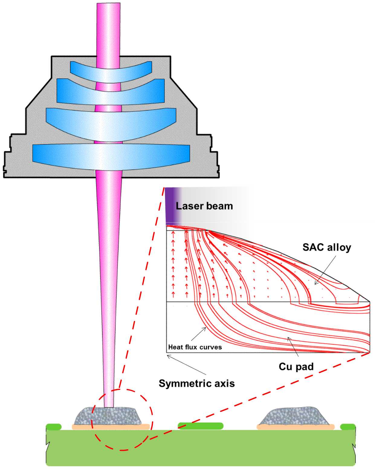
Fig 2. One of the result of the finite-element simulation: Heat fluxes and temperature gradients induced by laser beam.
A new, objective evaluation method is developed for characterizing the IML optical microscopic images of cross-sectional samples.
For the optical microscopic observation of IMCs a special sample preparation is needed. Since the contrast between the substrate and the IMC is usually low, the boundaries might be detected as blurred.
Thus a specific sample preparation method was established which separate the region of interest better than previously used methods (Fig 1.). The main idea of the method is that the OPS suspension generates trenches at the interface of the IMC and the solder, which causes high contrast in bright field illumination mode.
I have developed a sample preparation method based on selective electrochemical etching, which revealed the microstructure of the lead-free solder alloy.
The fine microstructure of the intermetallic network inside the solder bulk cannot be developed merely by chemical etching, since the uncontrolled reaction would probably damage the structure. A new selective electrochemical etching method was developed which can make the fine microstructure of the Ag3Sn inside the solder bulk visible (Fig 3.)

Fig. 3. During the selective etching the β-Sn is removed from the SAC305 solder, while the fine microstructure of the Ag3Sn intermetallic network remains intact.
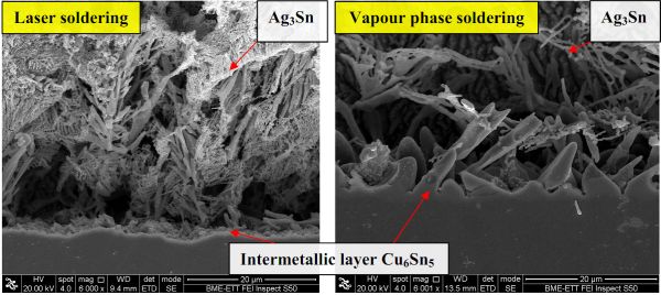
Fig. 4. SEM micrographs of the etched samples reflown by CO2 laser and vapor phased soldering device, near the IML
A quantitative measuring method is developed which can quantify the ratio of dissolved IMCs and pure thin in the solder bulk.
An experimental method was developed jointly with Mr. Attila Bonyár by which the ratio of the pure thin and the dissolved IMC can be measured. The method is based on the fact that the quantity of the etched tin is known because of the electrochemical setup. After the determination of etching depth the ratio can be calculated.
Expected impact
The result of my research has already been used in several industrial projects with significant success. The optimized cross-section preparation method is used daily in the failure analysis of electronic components at the Department.
We have already published two journal articles and a conference paper on the selective etching technique of which the conference paper gained the “Excellent oral award" at IEEE-ISSE2012.
The method is communicated directly to the industrial partners of our department and several cooperations for the practical application of the new test method is already in progress.
List of publications, reference list
List of publications
Revised, foreign-languages journals published in abroad
-
[L1] T. Hurtony, P. Gordon, B. Balogh, "Formation and Distribution of Sn-Cu IMC in Lead-Free Soldering Process Induced by Laser Heating”. MICRO AND NANOSYSTEMS 2:(3) pp. 178-184.
-
[L2] T. Hurtony, A. Bonyár, P. Gordon, G. Harsányi, "Investigation of intermetallic ompounds (IMCs) in electrochemically stripped solder joints with SEM”, MICROELECTRONICS AND RELIABILITY 52: pp. 1138-1142. (2012)
-
[L3] T. Hurtony, A. Bonyár, P. Gordon, "Microstructure comparison of soldered joints using electrochemical selective etching”, MATERIALS SCIENCE FORUM, in press. (2012)
-
[L4] E. Harkai, T. Hurtony, P. Gordon, "Effects of cooling rate on the acoustic properties of Pb-5Sn solder”, MATERIALS SCIENCE FORUM, in press. (2012)
Revised, journals in Hungarian
- [M1] Hurtony T., Bonyár A., Gordon P. "Ólommentes forrasz intermetallikus vegyületeinek karakterizálása” (in Hungarian), ELEKTRONET XXI:to be published (2012)
Foreign language international conference proceedings
-
[R1] T. Hurtony, "Simulation and modeling of laser ablation”, 31st International Spring Seminar on Electronics Technology, ISSE 2008 (IEEE). Budapest, Hungary, Budapest, pp. 452-457.
-
[R2] T. Hurtony, P. Gordon, B. Balogh, "Optimization of flip-chip laser soldering for low temperature stability substrate”, Microelectronics and Packaging Conference, EMPC 2009. Rimini, Italy, (IEEE), pp. 1-6
-
[R3] T. Hurtony, B. Balogh, D. Pintér, Gy. Lénárt, "Metallographic analysis of laser soldered chip resistors”, International Spring Seminar on Electronics Technology, ISSE 2010. Warsaw, Poland, (IEEE), pp. 123-127.
-
[R4] T. Hurtony, E. Harkai, P. Gordon, "Effect of solder pad symmetry on evolution of Sn‑Cu intermetallic compounds". XLVI International Scientific Conference on Information, Communication And Energy Systems and Technologies: ICEST 2011, Nis, Serbia, pp. 545-548.
-
[R5] T. Hurtony, B. Sinkovics, P. Gordon, "Characterization of microstructure of lead free solder by different image processing algorithms”, 17th International Symposium for Design and Technology of Electronics Packages, SIITME 2011. Timisoara, Romania, (IEEE) pp.327-331.
-
[R6] A.Bonyár. T. Hurtony, P. Gordon, "Selective electrochemical etching for the investigation of solder joint microstructures”, 35th International Spring Seminar on Electronics Technology. Salzburg, Austria, (IEEE), pp. 1-7.
-
[R7] E. Harkai, T. Hurtony, P. Gordon, "Inspection of Topography of Cracks Using Scanning Acoustic Microscopy”, XLVI International Scientific Conference on Information, Communication and Energy Systems and Technologies: ICEST 2011, Nis, Serbia, (IEEE), pp. 543-544.
Foreign language, national conference proceedings
-
[R8] L. M. Molnár, Sz. Dávid, T. Hurtony (Edited), Atomic Force Microscopy Investigations of Intermetallic Layers on Electronic Surface Finishings. Budapest, Hungary, 2010.
Link collection
Reference list
[1] Mathew Schaefer, Werner Laub, Janet M. Sabee, and Raymond A. Fournelle: A Numerical Method for Predicting Intermetallic Layer Thickness Developed During the Formation of Solder Joints, Journal of Electronic Materials, Vol. 25, No. 6, 1996
[2] Seo S-K, Cho MG, Choi WK, Lee HM, Comparison of Sn2.8Ag20In and Sn10Bi10In solders for intermediate-step soldering. J Electron Mater, 35 (2006), 1975–81.
[3] Kim DH, Cho MG, Seo S-K, Lee HM. Effects of Co Addition on Bulk Properties of Sn-3.5Ag Solder and Interfacial Reactions with Ni-P UBM, J. Electron. Mater. 38 (2009) 39-45.
[4] ChoMG, Kang SK, Shih DY, Lee HM. Effects of minor additions of Zn on interfacial reactions of Sn–Ag–Cu and Sn–Cu solders with various Cu substrates during thermal aging. J. Electron. Mater. 36 (2007) 1501–1509.
[5] B.S.S. Chandra Rao, J. Weng, L. Shen, T.K. Lee, K.Y. Zeng, Morphology and mechanical properties of intermetallic compounds in SnAgCu solder joints, Microelectronic Engineering 87 (2010) 2416–2422
[6] J. Keller, D. Baither, U. Wilke, G. Schmitz, Mechanical properties of Pb-free SnAg solder joints, Acta Materialia, 59 (2011) 2731–2741