 |
BMe Research Grant |

|

Doctoral School of Physics
Department of Atomic Physics
Supervisor: Erdei Gáborr
Optical Investigation of Detector Modules of Positron Emission Tomography
Introducing the research area
The 3 dimensional medical imaging has an important role in medical diagnostics and also in the research of metabolic processes, nervous system functions and evolution of tumor. An effective new device for these purposes is the combined magnetic resonance imaging (MRI) and positron emission tomography (PET). Such a new PET device should be built on new silicon technology based gamma detector modules. Building a new type of detector module poses a complex design, simulation and testing task on engineers to get the best optimized outcome. My aim is to develop a new measurement technology that makes the testing of detector modules easier. [1]
Brief introduction of the research place
The Optical Laboratory of the Department of Atomic Physics at the Budapest University of Technology and Economics carries out many optics related development jointly with industrial partners. Of the many partner companies, the Department completed several successful projects with Mediso Ltd. developer of pre-clinical and human medical imaging systems. Recently, this work has been carried out in the frame of a European consortium called SPADnet extending the scope of participant with universities and research centers.
History and context of the research
According to the basic principle of PET devices, a radioactive tracer is injected in the body so that the agent follows the spatial changes in the process they intended to investigate (Fig 1.). The radioactive tracer emits gamma photons, a pair at a time along a line and in opposite directions. By detecting these photons, and pairing them by their time of arrival, the set of line positions can be determined. From this set of lines the spatial distribution of radioactive tracer can be reconstructed using a mathematical transformation (Radon transformation).
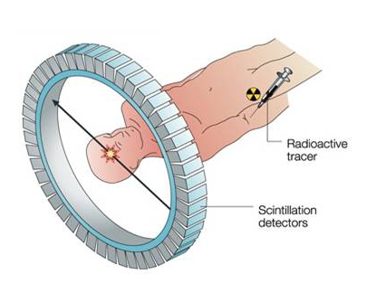
Figure 1. Basics of positron emission tomography
Conventional detector modules utilize scintillator crystals ordered in pin matrices that emit a few thousand photons by a gamma photon excitation. These photons are detected by photomultiplier tubes (PMT). The decoupling of these photons is completed by additional optical elements. Since PMTs cannot operate in the magnetic field of the MRI, manufacturers started developing new silicon based photomultipliers (SiPM) for future PET/MRI systems. [2, 3] These new sensors have further advantages, too. For example, they allow replacing the pin matrix with a continuous bulk crystal which is cheaper and makes positioning more accurate. In the testing of such detector modules, however, conventional measurement technology cannot be used.
The research goal, open questions
My aim is to develop a measurement technology capable of testing the new detector modules which are based on silicon technology with continuous crystal. A conventional test procedure utilizes a gamma beam to excite crystal pins along a line (Fig 2.). In this case, gamma photons excite crystal pins at various depths, therefore in the case of a single scintillation the position of excitation is unknown. In other words, we cannot identify the location of the single scintillation we're measuring. Yet, for a crystal pin acting as a homogenizer rod for optical photons this causes no problem. It means that even if we were able to see such low intensities, we would not be able to see a point source in a crystal, merely see the end of the rod lighting. In case of pin matrix we can conclude that the depth information of scintillation is lost.
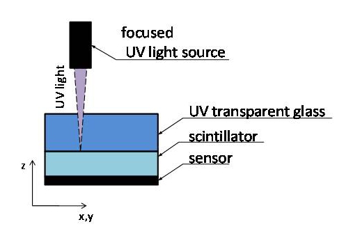
Figure 2. Testing method of the conventional PET module
What is good luck in the testing process is detrimental for the application. Losing the depth information causes the so called parallax error in the detection of the gamma photon propagation directions (or line of responses - LOR) (Fig 3.). If gamma emission occurs close to the edge of PET devices' field of view, then the line is not crossing the pin close to its axis but at a much wider angle. Consequently, it can cross multiple pins before being detected. In lack of depth information, this adds to the uncertainty of the LOR determination.

Figure 3. Effect of parallax error on the detection of photon emission's direction
In detector modules equipped with continuous crystals, light distribution detected by the sensor depends on the depth of gamma absorption. In its simplest case, the phenomenon of total reflection limits the angle of light that can escape the crystal. In this way, the spot size will depend on the depth of absorption, and consequently, the measurement technology discussed earlier cannot be applied. So we need to develop a technology capable of creating a point like excitation inside the crystal since we have to prove that light distribution changes with depth in more complicated optical arrangements. Also, we need to choose the proper light spot parameter (diameter, maximal intensity, etc.) suitable for depth estimations.
Methodology
Considering the physical laws governing gamma photon propagation we had to conclude that there is no way to carry out a point like excitation with them, and consequently, the crystal has to be excited in an alternative way. We have to emulate the response of the crystal to gamma photon absorption. While working out the emulation method, we have to consider several things as follows. In the emulated response, the spectral distribution of photons must be the same as in real case and the same applies to the number of emitted photons. Furthermore, light has to be generated in a small domain (in less than 0.1 mm diameter spherical volume). Finally, the duration of the process has to be the same as the real one which is 100-200ns.
It has been recently shown that the most widely used scintillator material the LYSO:Ce emits light with similar spectral distribution for both UV and gamma excitation. We base our process on this discovery. The idea is that we build up a sandwich made out of a glass with similar optical properties as the LYSO:Ce but transparent for the UV excitation and an LYSO:Ce layer. If we illuminate a sandwich like that through the glass and focus the excitation on the interface between the glass and scintillator then we going to get a point like excitation on this surface (Fig 4.). The optical properties of the two materials are the same, so the generated photons will propagate in the sandwich as if it were continuous.
Figure 4. Our measurement methodology for emulated continuous detector module
For the experimental realization of this experiment it is essential to prevent the passing of excitation light through the crystal because as it gets to the sensor it tampers the measurement. That is why at first we had to find a light (source) that is totally absorbed in the scintillator. For that we investigated the transmission of the scintillator, and as a result we chose a 365nm LED source. Considering these, we assembled an illumination optics capable of generating the tiny light spot of required size. When testing the manufactured optical setup, we found that the spectra of transmitted light contains a comparable amount of excitation light additionally to the excited light. We excluded this part of the illumination by using an additional filter. The LED is operated in a pulsed mode with a pulse length of 100-150ns, to get the realistic temporal behavior. The shape of the pulses were also verified by experiment. In order to prove the reliability of the method we built up the experiment that can be seen in Figure 5. We used a SensL SPM Array2 photon counter as sensor.

Figure 5. Draft of the experimental setup
Results
Process feasibility was completed in three steps. First, we verified that the optical properties of the glass in the emulated sandwich structure is really similar to those of the LYSO:Ce scintillator. This comparison was partly based on literature data, partly on our own measurements [5, 6]. We verified that the chosen Schott N-LASF44 type glass transmits the excitation light of the LED (Fig 6.). These tests and the investigations mentioned above could jointly prove that it was possible to find materials and technical solutions required for the realization of this kind of experiment.
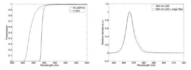
Figure 6. Transmission of the chosen glass material and the LYSO:Ce as a function of wavelength (left). Exciting light wavelength distribution with and without filter (right)
Next, we tested the properties of the chosen SPM Array2 sensor. Namely, we had to know whether this 4x4 pixel sensor has good enough pixel uniformity, and if not what correction factor had to be considered. The response of these sensors may not necessarily be linear with the incident light intensity, and then again, correction factors have to be determined for the consideration of this effect. Unfortunately, our measurements showed that the responses of the pixels are highly non-uniform, and therefore with the given setup it was not possible to measure the light distribution in full. As some pixels only produced their own noise, while others were already in saturation (Fig 7.), we decided using only the best pixel of the array. We measured different parts of the light distribution by placing that single pixel to different positions under the scintillator. Then we compiled the full light distribution measurement using these single pixel data. This method has the advantage of building arbitrary pixel arrays in this way. Its drawback of course, is the longer measurement time.

Figure 7. Sensitivity curve of some characteristic pixels as a function of incident photons
Considering all these, we prepared a 10x10x20mm3 detector module and covered its side faces with absorbing paint (Fig. 8). The module can be excited in two depths: 3 and 6 mm below the sensor surface. The crystal can be covered by a 3x6 element pixel array. In such an arrangement spot size is only determined by total reflection (Fig 9). As mentioned earlier, spot size depends on the depth of the scintillation in the crystal. This spot size can be calculated theoretically. By comparing the two values we got good agreement in case of both preset depths. With this measurement we verified that the captured light distribution was really coming from an emulated scintillation inside the crystal. [S1]

Figure 8. Emulated crystal module, excited in the middle

Figure 9. Intensity values measured on the middle pixel row in case of
3 (left) and 6 mm (right) below the sensor surface
Expected impact and further research
To complete the method there is one more step ahead of us. We have to determine the conversion factor between excited and emitted light intensities. Without this data absolute measurements cannot be done, only comparative ones.
With the assembled measurement setup in the future we can easily test any SiPM based detector module. Such an investigation may be beneficial for multiple reasons. It can be used to estimate the yield of light decoupling from the crystal and also the spatial resolution for various detector constructions. It can also serve as an intermediate step. If the sensor consists of large amount of pixels located in a small area (~50-100 pixels/cm2) than it is very important to find the proper method of reconstructing the position of the scintillation. For developers of such algorithms large amount of real light distribution data is valuable for the optimization of their process.
Publications, references, links
List of publications
[S1] G. Erdei, et al., "Refractive index measurement of cerium-doped Lux-Y2-xSiO5 single crystal," Optical Materials, Vol. 34., Issue 5, 2012, pp.781-785.
[S2] B. Játékos, et al., "Characterization of MRI-compatible PET detector modules by optical excitation of the scintillator material," SPIE Photonics Europe, 2012.
Links
BUTE, Department of Atomic Physics
BUTE, DAP, Medical Imaging Projects
References
[1] Zaidi H. "Recent developments and future trends in nuclear medicine instrumentation", Z Med Phys, 2006;16(1):5-17.
[2] P. Eckert, W. Shen, R. Stamen, and A. Tadday, “Characterisation Studies of Silicon Photomultipliers,” IEEE Jurnal of Quantum Electronics, vol. 44., No. 2., Febr. 2008, pp. 1-11.
[3] N. Dinu, “Electro-optical characterization of SiPM: A comparative study,” Nuclear Instruments and Methods in Physics Research Section A, vol. 610, Oct. 2009, pp. 423-426.
[4] L. Zhang, “Emission Spectra of LSO and LYSO Crystals,” IEEE Nuclear Science Symposium Conference Record, 2007.
[5] Schott AG., "Optical Glass Catalogue - Description of properties", online, 2011.