|
|
BMe Research Grant |
|
Doctoral School of Physics
Department of Physics/Institute of Physics
Supervisor: Dr. Szabolcs Csonka
Improvement of Cooper pair splitter nanocircuits
Introducing the research area
I study quantum effects arising in complex nanocircuits containing superconducting and normal phase conductors by means of electronic transport measurements. The goal of the research is to fabricate nanodevices capable of generating entangled electron pairs for the experimental investigation of quantum entanglement in the solid state and can initialize quantum bits in an entangled state in a quantum computer.
Brief introduction of the research place
Working in the research group of Dr. Szabolcs Csonka, I carry out the measurements in the Low Temperature Transport Laboratory of the Physics Department. The laboratory provides a unique background for low temperature measurements in the range of 4.2 K - 50 mK, enabling experiments in various fields of nanophysics.
The research is embedded in a wide international collaboration.
History and context of the research
Quantum entanglement, a quantum effect which manifests in surprising consequences [1], not only plays an influential role in fundamental physics, but also lies at the heart of quantum computation. Two particles are said to be in an entangled state when their two-particle wave function cannot be represented as a product of single-particle wave functions. Experiments with such entangled pairs of photons have already been carried out, demonstrating the violence of Bell’s inequality. However, similar experiments implemented in a solid state environment have not been implemented until now in lack of suitable devices capable of providing entangled electron pairs separated in space with an efficiency high enough [2].
Quantum computers store information in quantum bits. Quantum bits can be realized in any two-level quantum mechanical system, for example an electron spin [3]. Quantum algorithms can exceed the efficiency of their classical counterparts by taking advantage of the entanglement of quantum bits. If a device operating in a solid state quantum computer integrated in a chip is capable of generating entangled electron pairs, it can be used to initialize quantum bits in an entangled state and thus preparing them for quantum algorithms.
The research goal, open questions
Superconductors are natural sources of entangled electrons since their ground state is composed of spin-singlet electron pairs, the so-called Cooper pairs. These pairs can then be extracted from the superconductor via tunneling, their separation in space is enforced by the Coulomb interaction. Recently, nanocircuits capable of splitting Cooper pairs based on this principle have been realized, but their efficiency was rather low [4-5]. The goal of the research is to gain a deep understanding of the processes taking place in the Cooper pair splitter (CPS) circuit and fabricate new generation, high efficiency Cooper pair splitters to open up the route to the investigation of the entanglement of electron pairs.

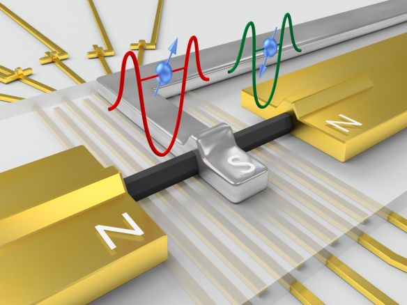
Figure 1 Artistic illustration of the new generation Cooper pair splitter. The hexagonal nanowire painted in black lies on an insulator layer, it is contacted with a superconducting electrode in the middle, and normal electrodes at the sides. An array of local gate electrodes below the insulator layer enables us to tune the chemical potential in the nanowire and form quantum dots.
Methods
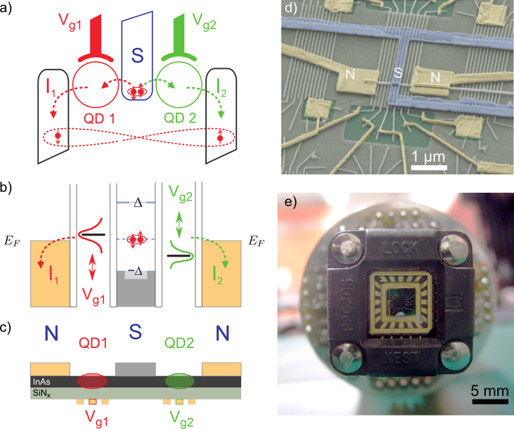
The CPS nanocircuit consists of a superconductor electrode coupled with two quantum dots and two normal leads (Fig. 2). Quantum dots (QD) are confined systems in which electrons populate states with discrete energy states whose spacing is determined by the Coulomb interaction. The transport process in which a Cooper pair leaves the superconductor and fills two states in the same QD is energetically unfavorable because of the Coulomb repulsion, and this principle provides the basis for the spatial separation. In the Cooper pair splitting process the electrons tunnel into different QDs and leave the circuit via the opposite normal leads. However, other transport processes also present, such as the sequential tunneling of electrons via the same QD, reduce the splitting efficiency.

Figure 2 a) Schematics of the CPS device [5]. b) Energy diagram of the CPS device in equilibrium. The Fermi energies EF of the normal leads coincide with the energy of the Cooper pairs. States below EF and the superconducting gap are filled completely. The levels of the QDs are tuned with the gate voltages Vg1 and Vg2. c) Simplified cross section of the nanostructure. QDs are formed in the indium arsenide (InAs) nanowire, the potential barriers confining the electrons are introduced by the local gate voltages. d) Artificially colored scanning electron micrograph of a CPS [S2]. e) The silicon wafer in the chip carrier.
Sample fabrication
The CPS nanocircuits are fabricated by means of electron beam lithography, the steps of the technique are illustrated on Fig. 3. We spin resist on a silicon wafer, then shine it with electrons in a scanning electron microscope, which makes the exposed resist area soluble in the developer solution. After development, we end up with a patterned resist mask, and depending on the selected fabrication step, we proceed with wet chemical treatment, dry etching or metal deposition by vacuum evaporation. The fabrication of next generation CPS devices requires four lithography cycles; starting with the creation of the array of local gates, next the patterned insulator layer, then using a micromanipulator the indium arsenide nanowire is placed on top of it and finally, we contact it with superconductor (niobium) and normal (titanium/gold) electrodes.
Figure 3 Steps of electron beam lithography (slide-show)
Measurement technique
The nanocircuits are characterized in a 3He-4He dilution refrigerator at a base temperature T~50 mK. Small signal measurements carried out at low temperatures raise several difficulties, namely, the electric lines are heavily filtered and we use standard lock-in technique to measure the small currents flowing in the nanocircuit. The superconducting vectormagnet built into the refrigerator can produce magnetic fields up to 3 Tesla in any direction of the plane, which allows suppressing superconductivity in the CPS and also to investigate anisotropic effects. The instruments are connected via GPIB and Ethernet to the PC which runs the program controlling them and visualizing measurement data in real-time.
Results
The phenomenon
The Cooper pair splitting process is demonstrated in a measurement as follows. After introducing potential barriers and having formed QDs in the nanowire, we tune the right QD to resonance. As long as the levels of the left QD are not aligned with the Fermi energy EF there is no current flowing in this arm, the QD is in Coulomb blockade. As we tune the levels and they cross the Fermi energy, the blockade is lifted and we can observe a finite current through the left QD as well. At the resonances of the left QD we can observe an increase in the current of the right QD, this is the sign of the phenomenon: at double resonance, the Cooper pair splitting becomes energetically favorable. When the superconductivity is suppressed with magnetic field, the positive contribution vanishes (see the dashed curve).
Figure 4 Experimental demonstration of the Cooper pair splitting. The graph shows the conductance of the left QD with red (scale to the left) and the right QD with green (scale to the right). Resonances of the left QD result in positive contributions in the current of the right QD, this is the sign of Cooper pair splitting.
The
first CPS devices lacked the local gate array and most device
parameters were incidental and not controllable. The gate array in the
new generation CPS devices enables the in-situ tunability of several
parameters, namely the QD-lead couplings. This way we could increase the
efficiency defined by
![]() from a few percentages beyond 30%.
from a few percentages beyond 30%.
Expected impact and further research
We have published our results in a leading journal with a high impact factor [S1], and presented a poster at a scientific conference [S2]. The publication summarizing our newest results is currently under preparation.
In the future we will enhance the nanostructure by using other superconducting leads (e.g. vanadium, tungsten-rhenium, lead) and in the long term we will conduct experiments with novel techniques to investigate the spin and entanglement of the split Cooper pairs.
Publications, references, links
Publications
[S1] L. Hofstetter, S. Csonka, A. Baumgartner, G. Fülöp, S. d’Hollosy, J. Nygård, and C. Schönenberger, Finite-Bias Cooper Pair Splitting, Phys. Rev. Lett. 107, 13680, 2011
[S2] S. d’Hollosy , G. Fülöp, A. Baumgartner, S. Csonka, M.H. Madsen, J. Nygård and C. Schönenberger, Electrical tunability of InAs nanowire quantum dots and Cooper pair splitting, poster presentation, Frontiers in Quantum Engineered Devices, 2013
[S3] Róbert Erdélyi, Morten Hannibal Madsen, György Sáfrán, Zoltán Hajnal, István Endre Lukács, Gergő Fülöp, Szabolcs Csonka, Jesper Nygård, János Volk, In-situ mechanical characterization of wurtzite InAs nanowires, Solid State Communications, 10/2012; 152(19):1829–1833
Fizipédia (in Hungarian):
Wikipedia:
Bell theorem (in Hungarian)
List of references
[1] A. Einstein, B. Podolsky, and N. Rosen, Can Quantum-Mechanical Description of Physical Reality Be Considered Complete?, Phys. Rev. 47, 777
[2] Waldemar Kłobus, Andrzej Grudka, Andreas Baumgartner, Damian Tomaszewski, Christian Schönenberger, and Jan Martinek, Entanglement witnessing and quantum cryptography with nonideal ferromagnetic detectors, Phys. Rev. B 89, 125404 (2014)
[3] J. R. Petta et al. Coherent Manipulation of Coupled Electron Spins in Semiconductor Quantum Dots. Science, 309:2180–2184 (2005)
[4] L. G. Herrmann et al. Carbon nanotubes as Cooper-pair beam splitters. Phys. Rev. Lett., 104(2):026801 (2010)
[5] L. Hofstetter, S. Csonka, J. Nygard, and C. Schonenberger. Cooper pair splitter realized in a two-quantum-dot Y-junction. Nature, 461:960–963 (2009)
