|
|
BMe Research Grant |
|

BME Doctoral School of Physics
Department of Physics/Institute of Physics
Supervisor: Dr. Mihály György
Experimental study of memristors
Introducing the research area
My research field covers the transport properties of nanometer-scale junctions embedded in insulating matrices. They are viewed as promising candidates for memory applications, due to their voltage-tunable conductivity [S1].
Brief description of the research place
My research work is carried out at the Solid State Physics Laboratory, where the majority of projects focus on nanotechnology, quantum transport, and molecular electronics. The laboratory is well-equipped for liquid helium and room temperature electrical transport measurements.
History and context of the research
The word memristor is an acronym derived from memory and resistor. The name refers to passive, two-terminal electrical circuit components, where the resistance depends on the current previously flown through the device. They show hysteretic current-voltage characteristics, and are widely applied in modeling bipolar resistance-change processes. The theoretical existence of memristors was first predicted by Leon Chua in 1971 [H1], and their experimental realization started in the early 2000’s [H2,H3].
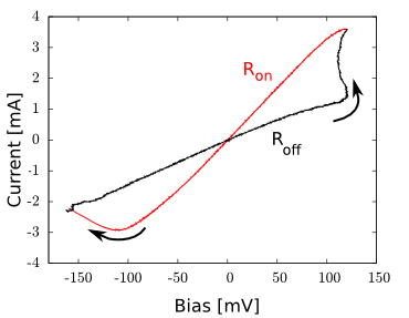
Figure 1: Specific current-voltage characteristic. This switching took place between Roff=70 Ω and Ron=30 Ω.
A typical current-voltage characteristic is shown in Figure 1. Increasing the bias from zero, one can measure the initial resistance of the junction (Roff). Further increase leads to some kind of a reconfiguration in the system. During a subsequent decrease of the bias, a linear dependence is observed again showing the on-state resistance Ron, until the negative threshold voltage is reached, where the initial resistance state is restored. Mapping the resistance states into bits, a computer memory can be constructed from these memristors. As the achievable resistance states are not limited to two, but vary on a wide scale, not only digital systems can be represented.
Memristors are prospective candidates for both computational applications and neural network modeling which explains for the increasing attention towards resistance-change processes. These devices not only approach the atomic size limit but also the time scale of GHz operation [S1], representing a promising basis for a future generation of high speed resistive switching memory devices overriding the downscaling limitations of current CMOS technology.
The research objectives, open questions

Figure 2: The evolution of a conducting filament in silver-sulphite placed between silver and electrochemically inert platinum electrodes [H4].
The development of the initial conducting filament in a silver-sulphite medium can be attributed to an electrochemical metalization process [H5]. In this model, the Ag2S is placed between an electrochemically inert and an active (typically silver) electrode, as illustrated in Figure 2. Upon suitable biasing conditions, the surface atoms of the silver electrode are ionized and migrate towards the surface of the inert electrode, where reduction and adsorption take place. This way a metallic filament builds up in the insulating silver-sulphite medium, constituting a conducting channel. These channels consist of silver atoms and silver-rich Ag2S islands as well [H6,H7]. In earlier studies, the complete formation and rupture of the filaments were investigated [H8] involving off state resistances higher than 1 MΩ. Such devices, however, can only operate at low switching speeds due to their fundamental RC limitations. Therefore, my research work focused on the resistance changes of the fully constructed filaments. The highly non-equilibrium processes dominating this regime had not been analyzed before.
During my research, I investigated the dynamics of switching from higher to lower resistances in devices utilizing Ag and PtIr electrodes. My task included determining the switching time, namely the shortest interval required to initiate non-volatile resistance changes and examination of the time dependence of the whole process, considering various bias parameters, like amplitude or frequency. The long-term stability of resistance states is of primary importance in terms of memory applications. Additionally, switchings were investigated as a function of temperature at different biasing conditions in order to reveal the dominating driving force behind the resistance change.
Methods
Sample preparation:
Ag thin films deposited on top of silicon substrate were sulphurised in low pressure atmosphere. Varying the sulphurisation time resulted in different silver-sulphite thicknesses built on top of the silver layer [H9]. The optimal thickness is around 30 nm; the contacts created on samples with thinner Ag2S layer proved unstable, while samples with higher silver-sulphite thickness showed semiconducting behavior.
Experimental techniques:
Most of the measurements were carried out in an STM (Scanning Tunneling Microscope) geometry, meaning that a mechanically sharpened tip was gently touched to the surface of the Ag-Ag2S heterostructure. High-precision positioning, outstanding mechanical and thermal stability is crucial for success because even a nanometer-scale shift can destroy the contact. The long-term exposure of samples to air is really harmful because silver thin films easily become oxidized, which leads to an insulating behavior. So the measurements were carried out in vacuum and the samples were stored in argon atmosphere. Moreover, special cabling were needed for reflection-less high-frequency measurements. These requirements were taken into account during the design of the room-temperature measurement setup, shown in Figure 3. Thermal stability was ensured by the thick copper walls of the chamber. To increase the mechanical stability, the setup was placed on top of a vibration isolation pad and the chamber was surrounded by a box covered by acoustically and thermally insulating material. The necessity of insulation is underlined by the fact that a mere one degree increase in temperature would lead to a thermal expansion sufficient to pull back the tip and break the contact.
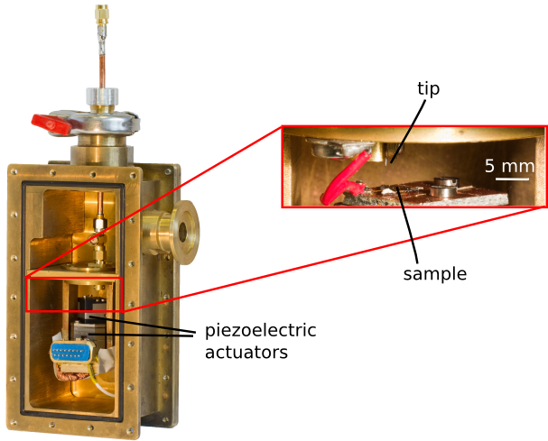
Figure 3 : The room temperature setup. With a tip fixed, contacts are created by positioning the sample using piezoelectric actuators bearing a nanometer-scale accuracy in each spatial direction.
To reveal the underlying physical phenomena of the observed resistive switching, temperature dependent measurements from cryogenic through room temperatures were conducted. A VTI (Variable Temperature Inset) was used for setting and monitoring environmental conditions. A VTI comprises a nitrogen shield and a helium bath separated from the environment by vacuum shields. The cooling of the sample is achieved by liquid helium, and a heater provided for the heating, which setup enabled varying the sample temperature in a wide range by the fine tuning the cooling and heating power.
Measurement control:
Measurement control programs were implemented in C# and Labview to achieve a fully automatic control of sample positioning and contact realization. Instrumental communication was also conducted via these programs along with the backup of measurement data and main instrumental settings. Data analysis was done by Matlab scripts designed for specific tasks.
Results
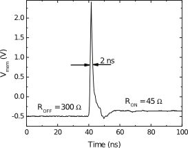
Figure 4 [S1]: Resistance change initiated by a single voltage pulse of 500 ps width and 2.5 V amplitude. The apparent 2 ns pulse width can be attributed to the limited detector bandwidth.
In my research work it was shown for the first time that the resistive switching of nanometer-scale metallic channels in silver-sulphite is a fast process taking place on a nanosecond time scale [S1]. A representative curve is shown in Figure 4, showing the relatively small Ron and Roff values inevitable for fast operation. Typical values of Roff/Ron ratios were as high as ~10 which satisfy the basic requirement to reliable read-out [H3]. Utilizing point contact Andreev reflection spectroscopy, the diameter and transparency of junctions could be determined. It was found that both ON and OFF states corresponded to truly nanometer-scale, highly transparent metallic channels [S1] which are far beyond the limitations of present day's lithographic techniques. In conclusion, it was demonstrated that these devices satisfy the requirements for future memory applications [H3].
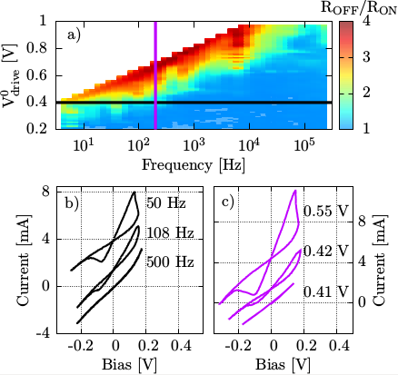
Figure 5 [S2]: a) Roff/Ron switching ratio as a function of driving amplitude and frequency. b) Curves measured at fixed 0.4 V amplitude and varying frequency. c) IV traces at a fixed 200 Hz frequency and increasing amplitudes.
Figure 5 a) shows the switching ratio as a function of the amplitude and frequency of the applied triangular voltage signal. Increasing the frequency at a fixed bias leads to smaller changes because the total charge flown through the device decreases (5 b)). Increasing the biasing amplitude at a fixed frequency increases the switching ratio (5 c)). The response to a constant driving bias applied on the junction and a series resistance can be understood similarly [S2]. The resistance change shows a highly non-exponential transition between the ON and OFF states, simultaneously exhibiting multiple time scales ranging from a nanosecond to seconds. This fundamental, inherent property of the Ag2S ionic conductor provides a unique opportunity for the combination of GHz write/erase operations performed at bias levels of a few volts, non-volatile read-out with slower signals of a few 10 mV and robust information storage at zero bias in a two-terminal, nanometer scale analog memory device. Additionally, the observed non-exponential behaviour along with the access to tunable multiple resistance states open a wide range of novel applications including integrated processing and storage platforms, multiple bit based computation schemes and improved neural network modeling
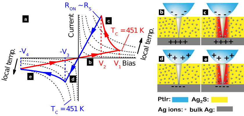
Figure 6 [S3]: a)Schematic illustration of the switching cycle at the I–V plane, with the characteristic Vbias voltages indicated. Along the dashed hyperbolae the I·Vbias dissipated power and the local temperature of the junction are constant. b) - e): Schematic illustration of the metallic filament. b) and d): low bias OFF and ON states, c) and e): elevated temperature at the vicinity of the filament accelerating the switchings.
More than ten thousands IV curves with varying series resistances were recorded in the range of 4.2 - 300 K in order to explore the physical phenomena responsible for resistance change [S3]. The data are in quantitative agreement with a model taking pronounced power dissipation released at the nanojunction’s length scale into account, giving rise to a local overheating of the junction up to the super-ionic phase transition of the Ag2S layer even at cryogenic ambient temperatures. This accelerates the field driven, thermally activated ionic migration processes as well as electrode reactions. The observed resistive switchings can be attributed to an enhanced filament reconfiguration accompanying the structural phase transition of the Ag2S matrix. In spite of the self-assembling nature of filament formation/destruction, the results demonstrate that these memory cells exhibit uniform behavior at technologically optimal device parameters.
Expected impact and further research
The high significance of presented results is confirmed by the big variety of possible applications ranging from fast and compact memory devices [H10] to novel neural network modeling schemes [H11]. Combining with other materials, the memristive behaviour can be beneficial in sensors, for example in light detectors [H12]. One can build logical gates out of memristors, therefore, the computational operations and data storage can be integrated on the same platform leading to a novel hybrid architecture.
In the future, I plan to create and investigate Ag - Ag2S -Ag junctions formed by electron beam lithography. This would greatly increase the stability, high-density integrability and applicability of the devices. Investigation of other materials such as silver-bromide is among my future plans as well. Further valued results could also expected from the investigation of the memory effect in materials exhibiting charge-density wave effects [H13].
Publications, references, links
Publications:
[S1]
A. Geresdi, M. Csontos, A. Gubicza, A. Halbritter and G. Mihály: Fast operation of nanometer-scale metallic memristors: highly transparent conductance channels in Ag2S devices, Nanoscale, 6, 2613 (2014)
[S2]
A. Gubicza, M. Csontos, A. Halbritter and G. Mihály: Non-exponential resistive switching in Ag2S memristors: a key to nanometer-scale non-volatile memory devices, Nanoscale, 7, 4394 (2015)
[S3]
A. Gubicza, M. Csontos, A. Halbritter and G. Mihály: Resistive switching in metallic Ag2S memristors due to a local overheating induced phase transition, Nanoscale, 7, 11248 (2015)
Links:
Scientific articles on memristors
References:
Leon O. Chua: Memristor - The Missing Circuit Element, IEEE Transactions on Circuit Theory, vol. ct-18, no 5. (1971)
D. B. Strukov, G. S. Snider, D. R. Stewart and R. S. Williams: The Missing Memristor Found. Nature Letters, 453, 80 (2008)
R. Waser, R. Dittmann, G. Staikov and K. Szot: Redox-based Resistive Switching Memories - Nanoionic Mechanism, Prospects and Challenges, Advanced Materials, 21, 2632 (2009)
K. Terabe, T. Hasegawa, C. Liang, and M. Aono: Control of Local Ion Transport to Create Unique Functional Nanodevices Based on Ionic Conductors, Science and Technology of Advanced Materials, 8, 536 (2007)
K. Terabe, T. Nakayama, T. Hasegawa and M. Aono: Formation and Disappearance of a Nanoscale Silver Cluster Realized by Solid Electrochemical Reaction, Journal of Applied Physics, 91, 12 (2002)
Z. Xu, Y. Bando, W. Wang, X. Bai and D. Goldberg: Real-Time In Situ HRTEM-Resolved Resistance Switching of Ag2S Nanoscale Ionic Conductor. ACS Nano, 4, 2515 (2010)
Z. Wang, T. Gu, T. Tada and S. Watanabe: Excess-Silver-Induced Bridge Formation in a Silver Sulfide Atomic Switch, Appl. Phys. Lett., 93, 152106 (2008)
T. Tamura, T. Hasegawa, K. Terabe, T. Nakayama, T. Sakamoto, H. Sunamura, H. Kawaura, S. Hosaka and M. Aono: Material Dependence of Switching Speed of Atomic Switches Made from Silver Sulfide and from Copper Sulfide, Journal of Physics: Conference Series 61, 1157 (2007)
A. Geresdi, A. Halbritter, E. Szilágyi, and G. Mihály: Probing of Ag-based Resistive Switching on the Nanoscale, MRS Proceedings, 1331 (2011)
J. J. Yang, D. B. Strukov and D. R. Stewart: Memristive Devices for Computing, Nature Nanotechnology 8, 13 (2013)
T. Ohno, T. Hasegawa, T. Tsukora, K. Terabe, J. K. Gimzewski and M. Aono: Short-term Plasticity and Long-Term Potentiation Mimicked in Single Inorganic Synapses. Nature Materials, 10, 591 (2011)
M. Aono and T. Hasegawa: The Atomic Switch, Proceedings of the IEEE, 98, 2228, (2010)
Kriza G, Mihaly G: Stretched-exponential Dielectric-relaxation in a Charge-density-wave System, Physical Review Letters 56, 2529 (1986)