|
|
BMe Research Grant |
|

Doctoral School of Physics
Department of Physics/Institute of Physics
Supervisor: Dr. Csonka Szabolcs
Ballistic Movement of Electrons in Suspended Graphene
Introduction of the research area
Graphene is one of the most intensively and most widely researched materials of the past decade. Its transparency, flexibility, high tensile strength and electric conductance all contribute to this. It consists of a hexagonal lattice of carbon atoms; such one atom thick layers build up graphite.
In most conductors, electrons are often scattered by atoms and lattice defects. However, the highest quality graphene samples show electrons travelling in a straight line along the full size of the sample (typically a few microns or tens of microns, scattering only on edges or electric contacts, like in billiard, thus Ohm’s law on specific resistance is not valid any more. The phenomena is called ballistic transport.
Ballistic electrons behave like light in many ways: they can be reflected, and can interfere with each other, which means that an analogue of a system of mirrors, lenses or optical fibres can be fabricated from graphene. This is the area of electron optics.
Brief introduction of the research place
Samples were prepared in Switzerland, with the University of Basel’s Nanoelectronics Group. Measurements took place both in Basel and in Budapest. Their group has a lot of experience in the fabrication of the highest quality suspended graphene samples. Researchers from our Department of Physics have worked together with them several times in the past in other research areas.
History and context of the research
Before the discovery of graphene in 2004, research on ballistic transport of electrons mostly confined to ultra-clean semiconductor structures, two-dimensional electron gases (2DEG). Unlike 2DEGs, the density (and thus the wavelength) of charge carriers can be tuned in a wide range in graphene. The special linear band structure of graphene makes its electrons, the so-called Dirac-electrons behave similar to the photons of light, or to relativistic particles (that move at velocities close to the speed of light). Analogues of relativistic phenomena can be observed, such as Klein-tunnelling: graphene’s electrons can pass through potential barriers with 100% probability even if the barrier is higher than the electrons’ energy. The analogue in classical physics would a ball getting through hill that it shouldn’t be able to get on top (roll over) in the first place.
The ballistic Dirac-electrons of graphene enable the observations of unique physical phenomena. Figure 1 displays a few interesting experiments in ballistic systems.

Figure 1 a) Electrons leaving contact 4 travel straight through graphene to contact 2, accumulating there, causing its voltage to drop. This can be observed even at room temperature.1, 2 b) Magnetic focusing: in a perpendicular magnetic field electrons follow circular cyclotron orbits. At certain magnetic fields, the end of a series of half circles will hit the neighbouring narrow electrode, initiating a voltage peak.3 c) Interference of electron waves: electrons reflected off contacts interfere with each other, similarly to the Fabry-Pérot effect. Depending on the ratio of wavelength and sample length, the waves interfere constructively or destructively, increasing or decreasing the total current.4, T1, T2
The research objectives, open questions
The goal of our research was to better understand ballistic Dirac-electrons. The required high cleanliness can be achieved by suspending graphene. To this end, a collaboration with researchers from Basel was established to optimize the special sample fabrication process.T3 The behaviour of ballistic electrons was studied in a simple setup, and p-n junction were created by bottom gate electrodes.
Graphene and the two bottom gates (the yellow electrodes on Figure 2) act as capacitor plates. By applying a positive voltage on the gates, the resulting electric field attracts electrons into the graphene strip above them, creating an excess of electrons, while a negative voltage causes the lack thereof, thus a positive charge density. By setting opposite voltages on the two bottom gates, the part of graphene located above the negative gate gains a positive density, while the part over the positive gate gains a negative charge density (p and n regions in Figure 6 a) ), similarly to a semiconductor p-n junction.
To understand the behaviour of electrons in the p-n junction, the current through the system was measured as a function of densities and magnetic field.
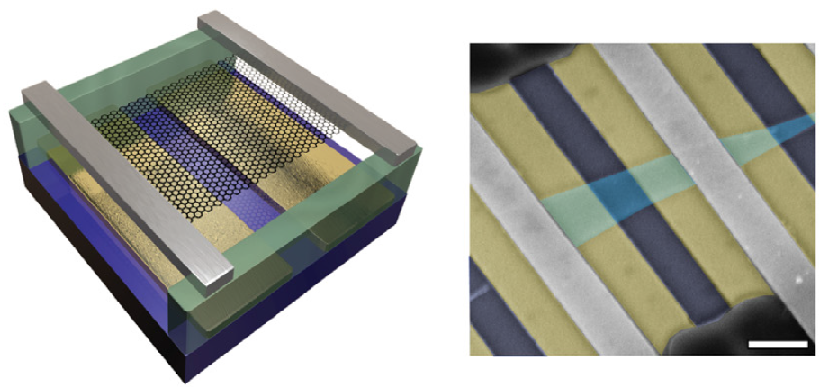
Figure 2 Schematic view and false-color scanning electron microscope image of graphene (turquoise) suspended from the contacts (gray) over bottom gate electrodes (yellow). Scale bar is 1 micron (µm). T3 Applying a negative voltage on one bottom gate, and positive on the other, the areas of graphene above them have positive (p side) and negative (n side) charge densities, respectively. Density changes from positive to negative over the middle (bluish) region.
Methods
Sample preparationT3
Ballistic transport can only be observed in high quality, ultra-clean samples. Graphene is usually deposited on a substrate, mostly silicon dioxide, but its charged impurities and lattice defects adversely effect the electrons of the graphene sample above, spoiling ballistic movement. Organic impurities that contaminate graphene itself can be removed by heating, using large current densities. However, certain fraction of heat is conducted away by the substrate, decreasing the efficiency of the annealing.
Best quality samples can be made by suspension, which eliminates the effect of substrate, and enables annealing to higher temperature.
In the first step, bottom gates are fabricated, using electron-beam lithography (EBL).
Figure 3 EBL: an insulating substrate is coated with a polymer (PMMA), and the chosen area is exposed to focused electron beam. The structure of PMMA changes, and can be dissolved using the proper chemical (development), so that the area becomes free of PMMA. A metal layer is deposited using thermal or e-beam evaporation, and after removing the polymer the metal remains only on the chosen area.
The wafer is then coated with a polymer (LOR), and the graphene is transferred on it (Figure 4). The contacts (wires) were created by lithography, and the LOR underneath graphene was exposed by e-beam lithography, finally, after a developing stage the graphene was suspended from the contacts.
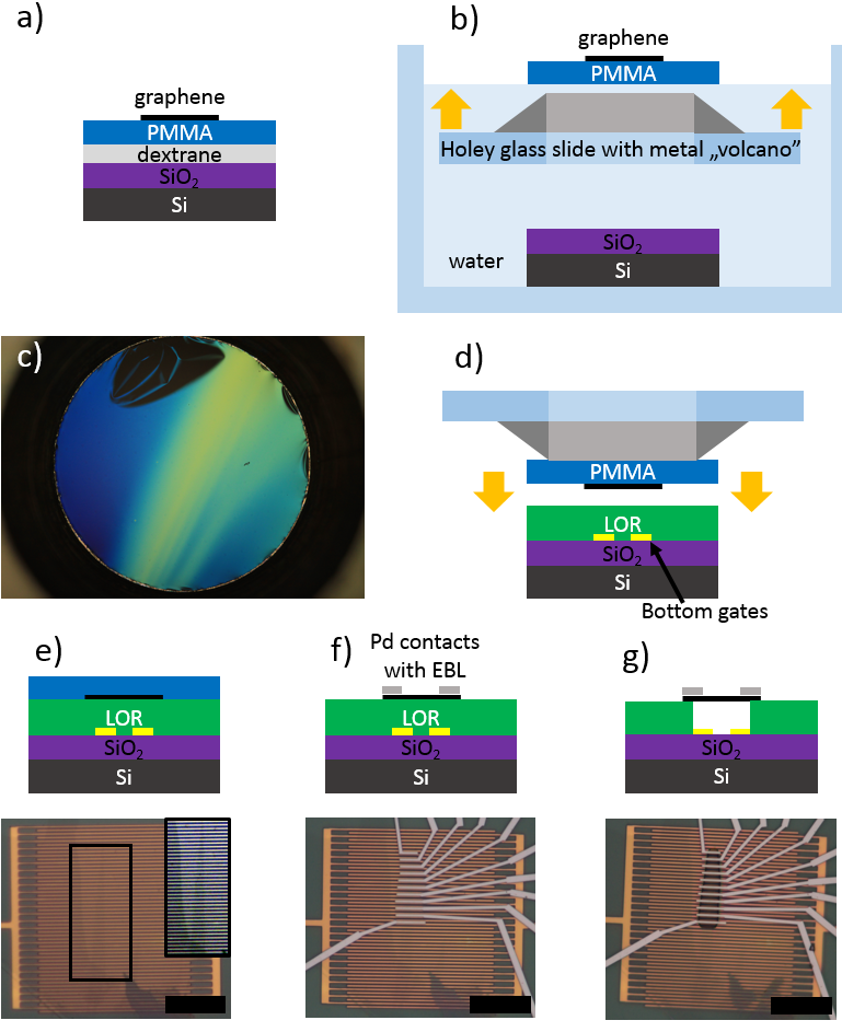
Figure 4 a) Graphene is made from graphite by exfoliation: a few layers was pulled off using sticky tape, and pressed on the surface. The small graphene flakes (on the scale of 10 µm) are located through an optical microscope, since their contrast is visible on the proper substrate, even though they are just one atom thick.5 It’s highly unlikely that such a small flake will happen to stick to the surface right above the bottom gates coated by LOR. Therefore, a temporary substrate was used instead, a double layer of dextrane and PMMA. b) Putting this in water the dextrane dissolves, and the PMMA membrane had to be fished for (with the graphene on top) with a 3 mm metal volcano on a holey glass slide. c) Photo of the volcano with the PMMA membrane. The dark smudge is actually a crease; graphene is not visible at this magnification. d) The volcano and PMMA were placed upside-down over the 0.6 µm thick LOR-coated bottom gates. Scale bar is 20 µm. e) The PMMA was dissolved, f) contacts (wires) were fabricated using EBL, g) LOR underneath the graphene was exposed and developed. Thus a graphene suspended from contacts over the bottom gates was obtained.T3
Method of measurement
Measurements were done in a cryostat at 1.5 K, to ensure that the electron energy and wavelength are well defined. To decrease the noise, Lock-in technique was applied, with 100 µV, and the current was measured via an amplifier.
Annealing
In order to remove the impurities, the (few-µm wide) sample was annealed with high, sometimes even 1mA/µm current density. The measurement presented below is from a sample that exhibited the quantized Hall effect at as low as 60 mT magnetic field, suggesting extraordinary quality after annealing.
Our results so farT2
The bottom gate voltages that create the p-n junction in opposite directions (Ṽ, -Ṽ) was changed, so the charge carrier densities proportional to the voltages (the densities of the parts of graphene above them) were also opposites (n, -n). Due to graphene’s special band structure the electron wave’s frequency is also reversed, and so is the group velocity.
In a perpendicular magnetic field B the Lorentz force, which is perpendicular to the electrons’ velocity, acts on the electrons, forcing them to follow circular cyclotron trajectories with radius Rc. By increasing B (or decreasing the density n) their diameter decreases below the sample size, so that the electrons leaving the wire bounce along the sample edge (Figure 5). Due to the direction-dependence of Klein tunnelling4, only the electrons arriving nearly perpendicularly at the p-n junction are transmitted. Rc is the same at the other side, but since Lorentz force is reversed due to the group velocity, they turn back to the p-n junction and, crossing it they again turn in the original direction, clockwise in the case of Figure 5. They snake over to the other edge of the sample in this manner, where they bounce along either to the left or to the right (Figures 6 a) and b) ), depending on how many half circles fit in the sample’s width W. Since the cyclotron radius changes with the density and field (Rc is proportional to |n|0.5/B), the electron will alternately go in this, then in the other direction with changing B or n. If it gets back to the source electrode or wire, it won’t contribute to the current, but if it goes to the drain, it will increase the current. This means that this snake state will probably manifest itself in an oscillating current. If we change B and n so that the cyclotron diameter (2Rc) remains constant, and it happens to fit in the width W even or odd times, we expect the current to be minimal/maximal, respectively; this means parabolae in the B-n plane (Figure 6 c) ).
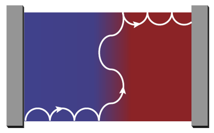
Figure 5 The electron propagating along cyclotron half circles turns in opposite directions (clockwise/counter-clockwise) on the sides of the p-n junction. It snakes along the junction over to the opposite edge, and goes on its way. T2
However, the problem is more complex, since the electrons that don’t arrive perpendicularly to the junction also get to the other edge of the sample: they are reflected off the p-n junction, and stay at the original p side, and bounce along the junction like they did on the lower edge before, and on the upper edge they can bounce over to the n side. What’s more, irregularities of the graphene edge might reflect the cyclotron trajectories depicted in Figures 5, 6 a), b) in a totally unpredictable, random way. All these might mask or ruin the current oscillations from snake states.
Figure 6 d) shows the colour-coded conductance map (which is proportional to the current) and its derivative with respect to the voltage Ṽ of one of the bottom gates, as a function of the voltage Ṽ and the magnetic field B. A pattern of oscillations is visible, which is similar to what we expected: conductance is minimal or maximal along parabolae that follow a constant ratio of cyclotron radius to width. This means that the contribution of snake states isn’t masked by other effects, and the picture described above matches the observed conductance oscillations.
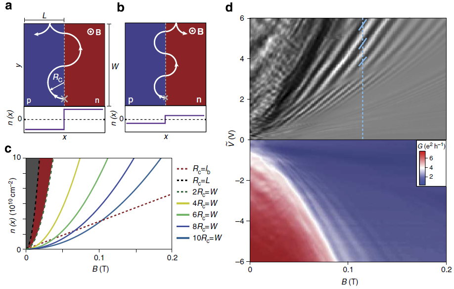
Figure 6 a), b) The snake state decreases or increases the current depending on the ratio of the cyclotron radius Rc and the sample width W. c) Rc is constant along the continuous lines shown here, and we expect the current and the conductance to be constant along them. d) Conductance (below) and its derivative (above) with respect to the bottom gate voltage Ṽ, as a function of Ṽ (which n is proportional to), and the magnetic field B. The pattern of conductance oscillations corresponds to the prediction of c). If a half circle is larger than the width, the oscillations disappear (2Rc>W) in the red and gray areas of c) ). But if Rc is smaller than the general width of the cyclotron trajectories (Rc<lB, right of the red dashed line), there are no cyclotron trajectories like we’ve described, and the oscillations vanish.T2
Expected impact and further research
Graphene is an excellent material for electron optics experiments, since ballistic transport is observable up to room temperature. 2 Due to the orientation-dependence of Klein tunnelling4, analogues of optical devices can be fabricated, such as a mirror or an optical fibre. After getting to know the behaviour of basic geometries we will be able to build larger systems for conducting more complex experiments. These pave the road for developing electron optics devices for applications, and also opens a new gate in nanoelectronics.
Graphene is also promising for spintronics devices, where the magnetic moment, or spin of electrons is utilized for data storage and logic operations. Ultra-clean graphene allows ballistic spintronics experiments, a world not yet discovered.
References
Corresponding publications of author:
[T1] M.-H. Liu, P. Rickhaus, P. Makk, E. Tóvári, R. Maurand, F. Tkatschenko, M. Weiss, C. Schönenberger, K. Richter: Scalable tight-binding model for graphene, Phys. Rev. Lett. 114, 036601 (2015)
[T2] P. Rickhaus, P. Makk, M.-H. Liu, E. Tóvári, M. Weiss, R. Maurand, K. Richter, C. Schönenberger: Snake trajectories in ultra-clean graphene p-n junctions, Nature Communications 6, 6470 (2015)
[T3] R. Maurand, P. Rickhaus, P. Makk, S. Hess, E. Tóvári, C. Handschin, M. Weiss, C. Schönenberger: Fabrication of ballistic suspended graphene with local gating, Carbon 79, p 486 (2014)
Other references:
[1] D.-K. Ki, A. F. Morpurgo: High-quality multi-terminal suspended graphene devices, Nano Letters, 2013, 13 (11), p 5165
[2] A. S. Mayorov, R. V. Gorbachev, S. V. Morozov, L. Britnell, R. Jalil, L. A. Ponomarenko, P. Blake, K. S. Novoselov, K. Watanabe, T. Taniguchi, A. K. Geim: Micrometer-scale ballistic transport in encapsulated graphene at room temperature, Nano Letters, 2011, 11 (6), p 2396
[3] T. Taychatanapat, K. Watanabe, T. Taniguchi, P. Jarillo-Herrero: Electrically tunable transverse magnetic focusing in graphene, Nature Physics 9, 225–229 (2013)
[4] P. Rickhaus, R. Maurand, M.-H. Liu, M. Weiss, K. Richter, C. Schönenberger: Ballistic interferences in suspended graphene, Nature Communications 4, 2342 (2013)
[5] P. Blake, E. W. Hill, A. H. Castro Neto, K. S. Novoselov, D. Jiang, R. Yang, T. J. Booth, A. K. Geim: Making graphene visible, Appl. Phys. Lett. 91, 063124 (2007)
[6] S. Morikawa, S. Masubuchi, R. Moriya, K. Watanabe, T. Taniguchi, T. Machida: Edge-channel interferometer at the graphene quantum Hall pn junction, Appl. Phys. Lett. 106, 183101 (2015)
[7] T. Stegmann, D. E. Wolf, A. Lorke: Magneto-transport along a boundary: from coherent electron focusing to edge channel transport, New J. Phys. 15, 113047 (2013)
Publication on an online Hungarian news portal:
http://index.hu/tudomany/2015/03/05/uttoro_grafenkutatasban_vettek_reszt_magyar_kutatok/
Other links in the text:
Mostly from Wikipedia.