|
|
BMe Research Grant |
|

Pálinkás András
BMe Research Grant - 2018
IIIrd Prize
![]()
Doctoral School of Physics
MTA, Centre for Energy Research Institute of Technical Physics and Materials Science
Supervisor: Dr. Osváth Zoltán
Preparation and investigation of graphene-metal nanoparticle hybrid nanostructures
Introducing the research area
Graphene1 is a truly two-dimensional, one atom thick layer of carbon. Due to its exceptional electronic and mechanical properties it shows promise for many technological applications such as flexible display screens or biochemical sensors [1]. Combining graphene with other materials can multiply its benefits by engineering the desired properties. The optical, electrical and chemical properties of nanoparticles2 made from metals or semiconducting materials may be different from those of their bulk counterparts. Graphene-metal nanoparticle hybrid materials potentially display not only the unique properties of metal nanoparticles and those of graphene, but also additional novel properties due to the interaction between graphene and nanoparticles. These new hybrid structures can have implications in the development of nanocomposites, sensors and possibly attract great interest in the field of chemical catalysis [2].
Brief introduction of the research place
My PhD work has been carried out under the supervision of Dr. Zoltán Osváth3 at the Institute of Technical Physics and Materials Science4, Centre for Energy Research5, Hungarian Academy of Sciences6 (MTA EK MFA). The Nanostructures Laboratory started to pursue graphene related research soon after the very first reports on graphene. Our group achieved several breakthroughs and made valuable contributions to this ever-emerging field of two-dimensional materials [3, 4].
History and context of the research
Novoselov and Geim isolated graphene in 2004 and demonstrated the new, rich physics it can offer [5]. We can understand the tremendous interest for graphene easily by considering the exceptional properties of this fascinating material. Its mechanical strength and flexibility [6], the high mobility of charge carriers [7], or its unusual electronic spectrum [8] are just a few of its interesting properties. Geim and Novoselov were awarded the 2010 Nobel Prize in Physics7 "for groundbreaking experiments regarding the two-dimensional material graphene".
Inspired by the preparation of graphene, a whole bunch of layered semiconductors, semimetals, insulators have been prepared in single atomic layer thickness, opening up new avenues for basic research and applications. The only common in these 2D-materials8 is the layered structure of their bulk form. While the atoms are connected to each other with strong chemical bonds within a layer, these materials can be easily exfoliated into single sheets thanks to the weakness of the van der Waals forces between the layers.
Owing to their 2D nature, the interaction with the environment, with the supporting material or with contacting nanoparticles is very important. As an example, graphene can inherit plasmonic or superconducting properties from contacting nanoparticles with such properties [9, 10]. On the other hand, both graphene’s chemical inertness and its impermeability make it favourable as a shielding layer for sensitive materials [11]. Understanding the interaction of graphene with its environment can open new pathways in the nanoscale engineering of graphene based hybrid materials.
The research goals, open questions
The goal of this research is to fabricate hybrid nanocomposites using graphene
and metal or semiconductor nanoparticles. The interaction between graphene and
other relevant materials in the field of nanotechnology, such as gold, tin and
SiO2 will be examined. It is crucial to understand the effect of
the environment on the properties of graphene, to unfold the mechanisms of the
possible doping and mechanical strain which may occur. In composite materials
the observable physical properties not only depend on the components
themselves, but also on the interaction between them.
The electronic structure of the graphene may be strongly affected by the
contacting metals; therefore, it is essential to engineer these contacts to
achieve the desired properties. To reveal possible charge transfer effects,
STS investigations will be performed on graphene supported by various metal
substrates. The properties of the prepared structures will be examined by AFM,
STM and Raman-spectroscopy, to unveil possible hazards, such as thermal or
environmental oxidation.
The surface plasmons9 on gold nanoparticles10 can be excited by laser. In resonance condition the exciting electromagnetic field can be enhanced by up to 11 orders of magnitude. Thanks to the surface-enhanced Raman scattering (SERS) very precise sensors can be fabricated, allowing for instance single-molecule detection [12]. If we add graphene onto these plasmonic structures, the chemisorption activity of the nanohybrid can be enhanced. I will study the resistance of the hybrid structure against high power laser irradiation.
Methods
In order to prepare graphene/nanoparticle hybrid nanostructures, firstly I had to prepare the nanoparticles on the desired substrate. Thanks to the wetting properties of the evaporated metals to each substrate materials, various structures can be formed. For instance, using SiO2 substrate a 5 nm thick, evaporated gold layer could be transformed to 15-20 nm height hemispheres by a subsequent heat treatment [13]. In contrary, the same gold film will be forced to form flat nanoislands with several hundreds of diameter if the substrate is the atomically smooth HOPG [P1]. We can achieve the same structures on the HOPG as on SiO2 if the graphite surface is roughened beforehand by Ar+ plasma treatment [13]. On the other hand the evaporated tin layer on the smooth HOPG self-organised to form nanoparticles [P4].
CVD-grown graphene was transferred onto the NPs using thermal release tape, and an etchant mixture consisting of a CuCl2 aqueous solution and hydrochloric acid. After the etching procedure, the tape holding the graphene was pressed onto the surface covered with nanoparticles. The sample stack was placed on a hot plate and heated to 95 °C, slightly above the release temperature of the tape.
Modern and complementary methods were used to examine the properties of the
graphene covered nanoparticles. I measured the morphology of the hybrid
structures with
Atomic Force
Microscopy11 (AFM) and
Scanning
Tunneling Microscopy12 (STM), with this latter not
only the sample’s topography, but also the electronic structure can be
detected. Scanning Tunnelling Spectroscopy (STS) was used to investigate how
the supporting nanoparticles influence the graphene’s Local Density of States
(LDOS).
Raman spectroscopy13
is a powerful and non-destructive tool for characterizing graphene, as the
number of the layers, the defects, the doping and the stress in graphene [14].
Results
Gold nanoislands were produced on HOPG surface from the evaporated 5-8 nm gold film by annealing, and then graphene was transferred onto the nanoislands. After a subsequent annealing at 650 °C I found that graphene induces surface re-crystallisation of the supporting gold nanoparticles, whereas the uncovered regions remained polycrystalline. Graphene on crystalline gold nanoislands exhibits moiré superlattices, which generate secondary Dirac points in the local density of states. The experimentally measured energies of these secondary Dirac points in graphene are well fitted with the expected theoretical dependence. Anomalously large wavelength moiré patterns and room temperature charge localization are observed. Such large wavelength moiré cannot be formed simply by the rotation misorientation of the atomic lattices. We showed by simulations that in such cases the graphene and the interfacial metallic layer is strained, leading to altered lattice constants in both graphene and the interfacial gold layer. [P1]
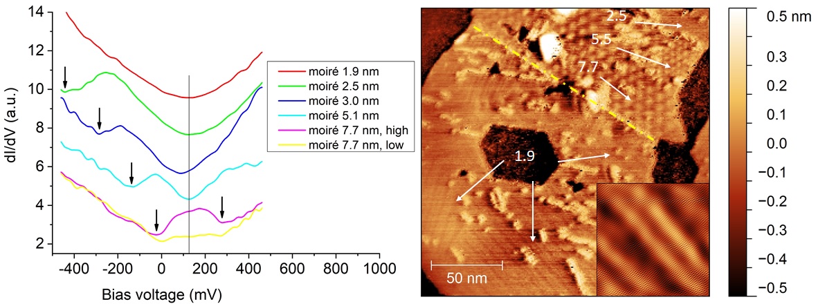
Figure 1. (a) Local density of states of graphene on Au (111) showing
superlattice Dirac points. Experimental dI/dV curves for different moiré
wavelengths: 2.5 nm (blue), 3.0 nm (magenta), 5.1 nm (orange), and 7.7 nm
(black and red). b) STM image of a hybrid graphene-gold nanocrystal after
annealing at 650 °C. Moiré superlattices of different wavelengths are
observed. [P1][Ref:
Carbon 107 792-799.
(2016)]
Sn NPs were prepared by evaporating 7 – 8 nm tin on HOPG substrates, which
self-organised into nanoparticles. Graphene was transferred on top of the tin
NPs immediately after evaporation. The graphene is impermeable to all gases
therefore it can be used as a protecting layer for sensitive metals. The
shielding efficiency of graphene is demonstrated, it is found to protect the
underlying tin NPs. I showed by STM and STS that tin NPs reduce significantly
the environmental p-type doping of graphene. Furthermore, with the help of our
colleagues in Košice we could demonstrate by low-temperature STM and STS
measurements that superconductivity is induced in graphene, either directly
supported by Sn NPs or suspended between them. Additionally, we prepared SnOx
NPs by annealing the evaporated tin at 500 °C, before transferring graphene on
top of them. The one atom thick covering layer anchors these semiconducting
NPs to the surface, making possible to investigate them by STM. STS
measurements performed on hybrid graphene/SnOx nanostructures
reveal the wide electronic band gap of SnOx NPs (≈3 eV). [P4]
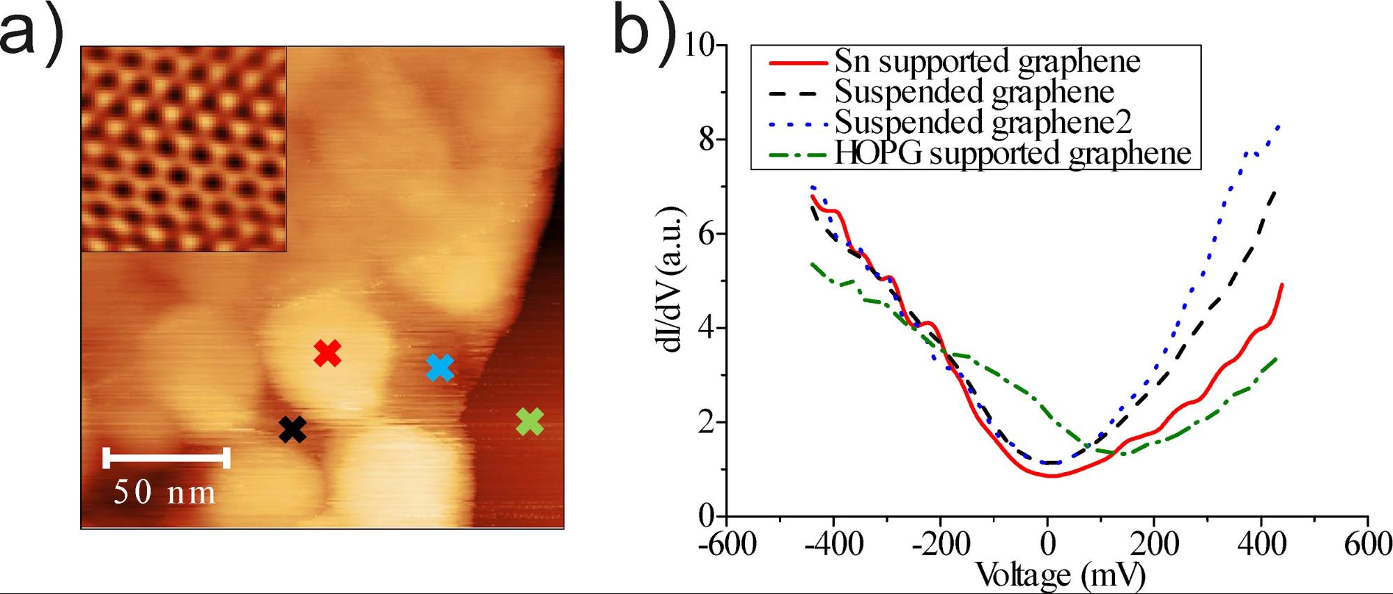
Figure 2. STM and STS investigation of graphene/Sn NPs. (a) STM topography of
graphene covered areas measured at T = 300 K. Atomic resolution images of Sn
supported graphene are shown in the inset. (b) STS spectra measured at T = 300
K. [P4][Ref.:
Carbon 124 611–617.
(2017)]
Gold NPs were prepared on SiO2 substrate by local annealing of gold thin films using focused laser beam. I transferred graphene onto these NPs with the same method as above. As a control experiment, graphene was transferred onto clean SiO2 substrate as well. I performed subsequent Raman-spectroscopy measurements on the samples with different laser powers. Low intensity was used for monitoring the doping and stress in graphene. In addition, between the low-power rounds I used high intensity laser to locally heat the sample. While I found that successive higher intensity (6 mW) laser irradiation increased gradually the doping and the defect concentration in SiO2 supported graphene, the same irradiation procedure did not induce such irreversible effects in the graphene supported by gold NPs. Moreover, the laser irradiation induced dynamic hydrostatic strain in the graphene on Au NPs, which turned out to be completely reversible. This latter finding can be explained with the different thermal expansion coefficients, which is positive for gold and negative for graphene. As far as I know, all reported measurements on graphene’s resistance against laser irradiation were performed with standard SiO2 as supporting material. Nevertheless, as I pointed out also above, the role of the substrate and the possible occurring of water film cannot be neglected. [P5]
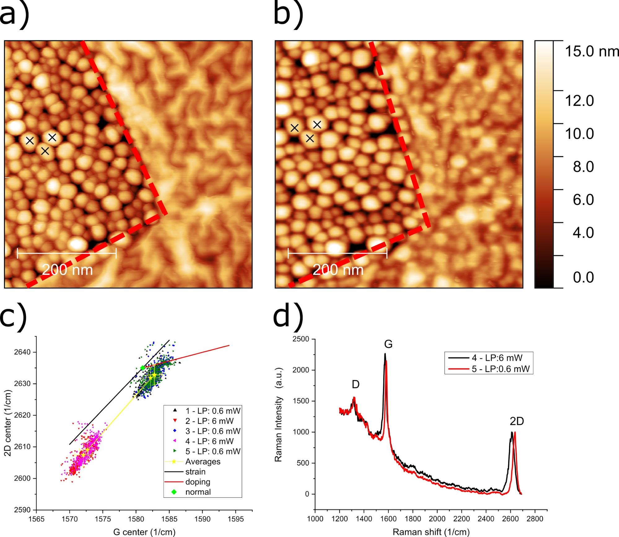
Figure 3. (a) and (b) AFM topography image of the sample before and after high
intensity laser irradiation. (c) 2D-G correlation plots of Raman peak
positions of the Au NPs supported graphene. (d) Average spectra measured with
low- (red) and high (black) laser power. Note, that the spectra are normalised
to the 2D peak intensity. [P5][Ref.:
Nanoscale (2018), doi:
10.1039/C8NR02848F]
Expected impact and further research
Devices based on graphene covered gold nanoparticles are prominent candidates for sensors utilizing the SERS effect, with single-molecule detection capabilities. The applied laser intensity should be carefully set with respect to preserving device integrity and a good signal-to-noise ratio. Our findings on the temperature related effects, such as surface recrystallization and oxidation can have implications in the development of graphene/nanoparticle based devices.
I
plan to investigate the resistance of graphene against laser irradiation on
various substrates with different wetting properties. Furthermore, novel
hybrid nanostructures based on graphene and other metals (eg. silver) will be
prepared and investigated.
Publications, references, links
List of corresponding own publications
[P1] A. Pálinkás, P. Süle, M. Szendrő, Gy. Molnár, C. Hwang,
L. P. Biró and Z. Osváth
Moiré superlattices in strained graphene-gold hybrid nanostructures,
Carbon 107 792-799. (2016) doi:
10.1016/j.carbon.2016.06.081
[P2] A. Pálinkás, Gy. Molnár, Chanyong Hwang, L. P. Biró and
Z. Osváth
Determination of the STM tip-graphene repulsive forces by comparative STM and
AFM measurements on suspended graphene,
RSC Advances 6 pp. 86253-86258. (2016) doi:
10.1039/C6RA19660H
[P3] I. Hagymási, P. Vancsó, A. Pálinkás and Z. Osváth
Interaction effects in a chaotic graphene quantum billiard
PHYS. REV. B 95:(7) 075123. (2017) doi:
10.1103/PhysRevB.95.075123
[P4] A. Pálinkás, Gy. Molnár, G. Z. Magda, C. Hwang, L.
Tapasztó, P. Samuely, P. Szabó and Z. Osváth
Novel graphene/Sn and graphene/SnOx hybrid nanostructures: induced
superconductivity and band gaps revealed by scanning probe measurements
Carbon 124 611–617. (2017) doi:
10.1016/j.carbon.2017.09.026
[P5] A. Pálinkás, P. Kun, A. A. Koós and Z. Osváth
Dynamic strain in gold nanoparticle supported graphene induced by focused
laser irradiation
Nanoscale (2018) accepted doi:
10.1039/C8NR02848F
List of other publications
1. Pálinkás András, Molnár György, Osváth Zoltán:
Grafén/arany hibrid nanoszerkezetek vizsgálata pásztázó alagútmikroszkópiával
Tavaszi Szél 2016. Tanulmánykötet. I. kötet. pp. 274-288. (2016)
Budapest, Doktoranduszok Országos Szövetsége
(ISBN:978-615-5586-09-6)
2. A. Pálinkás, P. Süle, Gy. Molnár, C. Hwang, L. P. Biró
and Z. Osváth
Investigation of graphene-gold hybrid nanostructures by scanning tunnelling
microscopy and spectroscopy
7th Szeged International Workshop on Advances in Nanoscience SIWAN 7., Szeged
(2016)
(ISBN:978-963-05-9801-9)
Table of links.
1.
https://en.wikipedia.org/wiki/Graphene
2.
https://en.wikipedia.org/wiki/Nanoparticle
3.
http://www.energia.mta.hu/~osvath/
4.
https://www.mfa.kfki.hu/
5.
http://www.energia.mta.hu/
6. http://mta.hu/
7.
https://www.nobelprize.org/nobel_prizes/physics/laureates/2010/
8.
https://en.wikipedia.org/wiki/Two-dimensional_materials
9.
https://en.wikipedia.org/wiki/Plasmon
10.
https://www.sigmaaldrich.com/technical-documents/articles/materials-science/nanomaterials/gold-nanoparticles.html
11.
https://en.wikipedia.org/wiki/Atomic_force_microscopy
12.
https://en.wikipedia.org/wiki/Scanning_tunneling_microscope
13.
https://en.wikipedia.org/wiki/Raman_spectroscopy
List of references
1. E.P. Randviir, D.A.C. Brownson, C.E. Banks, A decade of graphene research: production, applications and outlook, Mater. Today 17 (2014) 426–432. doi:10.1016/j.mattod.2014.06.001
2. I. Khalil, N.M. Julkapli, W.A. Yehye, W.J. Basirun, S.K. Bhargava, Graphene-gold nanoparticles hybrid-synthesis, functionalization, and application in a electrochemical and surface-enhanced raman scattering biosensor, Materials 9 (2016) 406. doi:10.3390/ma9060406.
3. G.Z. Magda, X. Jin, I. Hagymasi, P. Vancso, Z. Osvath, P. Nemes-Incze, C. Hwang, L.P. Biro, L. Tapaszto, Room-temperature magnetic order on zigzag edges of narrow graphene nanoribbons, Nature. 514 (2014) 608–611. doi:10.1038/nature13831.
4. L. Tapasztó, T. Dumitrica, S.J. Kim, P. Nemes-Incze, C. Hwang, L.P. Biró, , Breakdown of continuum mechanics for nanometer wavelength rippling of graphene, Nat. Phys. 8 (2012) 1–14, doi:10.1038/nphys2389.
5. K.S. Novoselov, A.K. Geim, S.V.S. Morozov, D. Jiang, Y. Zhang, S. V. Dubonos, I. V. Grigorieva, A.A. Firsov, Electric field effect in atomically thin carbon films, Science 306 (2004) 666–669. doi:10.1126/science.1102896.
6. C. Lee, X. Wei, J. Kysar, J. Hone, Measurement of the elastic properties and intrinsic strength of monolayer graphene, Science 321 (2008) 385–8. doi:10.1126/science.1157996.
7. K.I. Bolotin, K.J. Sikes, Z. Jiang, M. Klima, G. Fudenberg, J. Hone, P. Kim, H.L. Stormer, Ultrahigh electron mobility in suspended graphene, Solid State Commun. 146 (2008) 351–355. doi:10.1016/J.SSC.2008.02.024.
8. Geim, A. K. & Novoselov, K. S. The rise of graphene. Nature Materials 6, 183–191 (2007) doi:10.1038/nmat1849
9. Z. Fang, Y. Wang, Z. Liu, A. Schlather, P.M. Ajayan, F.H.L. Koppens, P. Nordlander, N.J. Halas, Plasmon-induced doping of graphene, ACS Nano. 6 (2012) 10222–10228. doi:10.1021/nn304028b.
10. A. Allain, Z. Han, V. Bouchiat, Electrical control of the superconducting-to-insulating transition in graphene-metal hybrids, Nat. Mater. 11 (2012) 590–4. doi:10.1038/nmat3335.
11. V. Berry, Impermeability of graphene and its applications, Carbon 62 (2013) 1–10. doi:10.1016/j.carbon.2013.05.052.
12. S. Nie, S.R. Emory, Probing single molecules and single nanoparticles by surface-enhanced Raman scattering, Science 275 (1997) 1102–1106. doi:10.1126/science.275.5303.1102.
13. Z. Osváth, A. Deák, K. Kertész, G. Molnár, G. Vértesy, D. Zámbó, C. Hwang, L.P. Biró, The structure and properties of graphene on gold nanoparticles, Nanoscale 7 (2015) 5503–5509. doi:10.1039/C5NR00268K.
14. A.C. Ferrari, D.M. Basko, Raman spectroscopy as a versatile tool for studying the properties of graphene, Nat. Nanotechnol. 8 (2013) 235–246. doi:10.1038/nnano.2013.46.