|
|
BMe Research Grant |
|

Rácz Adél Sarolta
BMe Research Grant - 2018
![]()
George A. Olah Doctoral School of Chemistry and Chemical Technology
MTA EK MFA, Thin Film Physics Laboratory
Supervisor: Dr. Sulyok Attila
Design of Corrosion Resistive SiC Nano-Layers
Introducing the research area
Silicon-carbide (SiC) has many advantageous properties such biocompatibility, high heat resistance, high wear resistance, good thermal conductivity and high corrosion resistance. Therefore, among others SiC is used in micro/nano-electromechanical systems (MEMS/NEMS), which are operating in harsh environments e.g. automotive and aerospace applications such as combustion processes or gas turbine controls [1-4]. Its production requires high temperatures but certain substrates do not bear elevated temperatures. Therefore, I investigated whether it is possible to produce thin SiC layer at room temperature. It turned out that the problem can be solved by ion mixing; I produced tens of nanometers thick SiC by a technology which is scalable up to wafer size.
Brief introduction of the research place
I work with the contribution of Dr. Miklos Menyhard in MTA EK MFA, in the Thin Films Physics Laboratory. The main strength of our laboratory is transmission electron microscopy and different surface sensitive spectroscopic techniques.
History and context of the research
The protection of sensors is essential. In many cases SiC protective layers are used because of its previously mentioned advantageous properties. Its production needs high temperatures which might be disadvantageous by certain substrates. However, by means of ion irradiation it is possible to produce compounds with high heat of formation. Formerly for these purposes high energy ions were applied [5]. Decreasing the ion energy, thinner – some nanometers thick - layers can be created which are located close to the surface. Recently in our laboratory we have succeeded to produce SiC at room temperature, applying focused ion beam method (FIB) by irradiating C/Si (10-20 nm) multilayer structures with gallium ions [6]. Its disadvantage was that it is quite costly and is not feasible for irradiating macroscopic areas, thus is not appropriate for production of protective layers. Therefore, it is advisable to examine whether the FIB method can be replaced by other ion bombarding method. I investigated the possibility of noble gas irradiation.
The research goals, open questions
During my work I investigated 4 problems.
a. The dependence of SiC formation of the parameters of noble gas irradiation.
Hence, I changed the projectile, the fluence, the energy of the mixing ion and the layer structure.
b. The characterization of the chemical resistance of the formed layer and finding a possible correlation between the irradiation parameters and the chemical resistance.
c. The description of the effect of ion irradiation also by simulation techniques. It helps designing protecting layers and speeds up the process.
d. Creation of SiC nanostructures in one step. By applying a masking layer compound formation and creation of nanostructured SiC takes place simultaneously.
Methods
a. Three different C/Si multilayer structures have been irradiated by xenon and argon ions at room temperature. The applied energies were between 40-120 keV, the applied fluences between 0.25-6x10¹⁶ ion/cm2. The multilayers differed in the layer thicknesses (10-20 nm) and successions. The system was built by magnetron sputtering. I examined the SiC formation by Auger electron spectroscopy (AES) depth profiling which could be detected by the change of the carbon and silicon Auger peaks. Fig.1 shows this phenomenon through the Auger peak of carbon. We can see that the peak can be decomposed and is a simple sum of the SiC and graphite spectra. I calculated the amount of SiC and its in-depth distribution from the AES depth profiles.
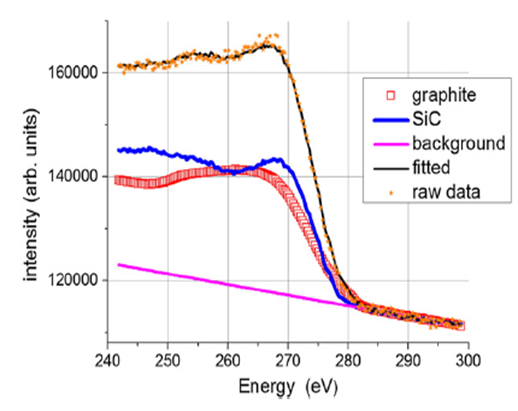
Figure 1: Auger spectra of carbon and its peak decomposition [7]
b. For characterizing the chemical resistance of the layers I performed potentiodynamic corrosion test in 4M KOH solution from which I could determine the corrosion rate of the samples.
c. For predicting the effect of irradiation I applied the TRIDYN simulation software. This program describes the ion mixing of Si and C layers very well, thus we can get the in-depth distribution of the Si, C and mixing ion, from which the amount of SiC can be calculated by applying a simple rule.
d. For creating the nanostructures I applied two different masking layers, one was a Langmuir-Blodgett film made from silica particles (diameter 590 nm), the other a grid of a periodicity of 2 µm. After the irradiation the mask and the non-irradiated part was removed by etching in microwave plasma and in HF/HNO3 solution. The structures were characterized by atomic force microscopy.
Results
a. I have shown how we can tune the in-depth distribution of SiC by changing the irradiation parameters (fluence, energy) and the layer structure. The applied energy determines the penetration depth of the mixing ion. The fluence determines the number of penetrating ions, in fact the formed amount of SiC. Fig. 2b shows as an example the effect of 6x10¹⁶ Ar+/cm2, 40 keV irradiation, Fig. 2a presents the AES depth profile of the non-irradiated sample for comparison where we can see that all interfaces are sharp. However, the irradiation caused SiC formation at the C/Si interfaces. We can see that less SiC is formed at the 2nd C/Si interface, than at the first one which is attributable to the 40 nm penetration depth of argon ions [8]. Fig. 2c shows an irradiation where we managed to create a continuous SiC distribution.
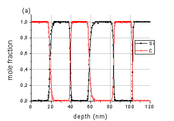

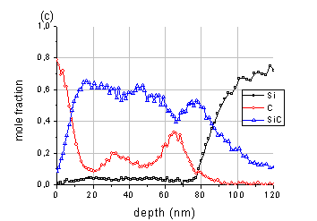
Figure 2.
AES depth profiles a. non-irradiated b. irradiated (6x10¹⁶ Ar+/cm2,
40 keV)
c. irradiated (3x10¹⁶ Xe+/cm2, 120 keV)
samples
b. The corrosion tests performed on differently irradiated samples have shown that the measured corrosion current density depends on the amount of SiC and that the corrosion resistance of as low as some nanometers thick SiC-rich layer is significantly higher than that of silicon. By introducing a new quantity, the effective areal density of SiC – calculated from the AES depth profiles – I managed to find a connection between the ion mixing and the corrosion property of the formed layer (Fig. 3). We hope that by choosing the proper irradiation conditions the chemical resistance of the layers can be tailored. [S1-S2].
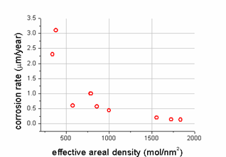
Figure 3: The corrosion rate vs. effective areal density of SiC for all measured data
c. I have shown that by applying fast and cheap simulation techniques the design of corrosion resistant layer is possible [S3]. We learned from previous research that the TRIDYN simulation describes the mixing of C/Si system very well. Calculating the depth profiles of all irradiations, extracting the effective areal densities of SiC and plotting them as a function of the measured corrosion rates we get a curve similar to what we get in the case of Auger spectra. (Fig. 4).
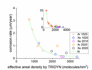
Figure 4: The corrosion rate vs. effective areal density of SiC for all measured data, inset, and enlarged y axis.
d. We can say that the creation of nanostructures in one-step was successful. Fig. 5 shows AFM pictures of the different patterns. It can be seen that we succeeded to produce quasi periodic 2D structures. By applying appropriate mask one can create any type of structures. I have also shown by AES depth profiling that in the irradiated region – unprotected by mask – SiC-rich region was produced [S4].
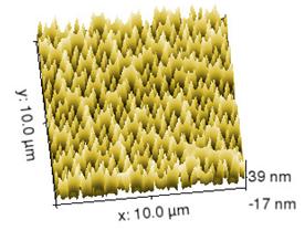
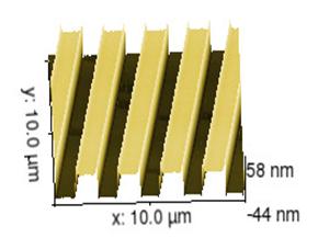
Figure 5: SiC nanopatterns with different masking layers a. silica particles 590 nm b. grid 2 µm
Expected impact and further research
It is possible that our method developed for producing SiC protective layers will be used for replacing diamon-like carbons (DLC) applied in MEMS. The importance of the research is proved by two articles published in the prestigious ACS journal, and a further one is in preparation. In the future it would be worthy to check whether ion mixing can be used for producing protective layers made of other high heat of formation compounds.
Publications, references, links
List of corresponding own publications
[S1]A.S. Racz, Z. Kerner, A. Nemeth, P. Panjan, L. Peter, A. Sulyok, G. Vertesy, Z. Zolnai, M. Menyhard: Corrosion resistance of nano-sized SiC rich composite coatings produced by noble gas ion mixing, ACS Appl. Mater. Interfaces, 2017, 9 (51), pp 44892–44899. IF=7.504
[S2]Rácz Adél Sarolta: Szilícium-karbidban gazdag nano-védőréteg előállítása nemesgázokkal történő ionkeveréssel, Tavaszi Szél konferencia-kiadvány, 2017, pp.120-129
[S3] A. S. Racz, M. Menyhard Design of corrosion resistive SiC nano-layers ACS Appl. Mater. Interfaces, 2018, DOI: 10.1021/acsami.8b06425
IF=7.504
[S4] A. S. Racz, D. Zambo, Z. Zolnai, G. Dobrik, A. Deak, M. Menyhard Novel methods for SiC nanopatterns, in preparation
Table of links
https://en.wikipedia.org/wiki/Silicon_carbide
https://en.wikipedia.org/wiki/Nanoelectromechanical_systems
https://en.wikipedia.org/wiki/Transmission_electron_microscopy
http://www.chem.qmul.ac.uk/surfaces/scc/scat5_2.htm
https://www.mee-inc.com/hamm/electrochemical-corrosion-testing/
http://www.hzdr.de/db/Cms?pOid=21578&pNid=0
https://en.wikipedia.org/wiki/Langmuir%E2%80%93Blodgett_film
https://www.nanoscience.com/technology/afm-technology/how-afm-works/
https://en.wikipedia.org/wiki/Diamond-like_carbon
List of references
[1] Sarro, M. Silicon carbide as a new MEMS technology. Sens. and Act. 2000, 82, 210-218.
[2] Maboudian, R.; Carraro, C.; Senesky, D.G.; Roper, C.S. Advances in silicon carbide science and technology at the micro- and nanoscales. J. Vac. Sci. Technol. A 2013, 31, 50805–50818.
[3] ) Phan, H. P.; Cheng, H. H.; Dinh, T. K.; Wood, B.; Nguyen, T. K.; Mu, F.; Kamble, H.; Vadivelu, R.; Walker, G.; Hold, L.; Iacopi, A; Haylock B.; Dao, D.V.; Lobino, M.; Suga, T.; Nguyen, N.T. Single crystalline 3C-SiC anodically bonded onto glass: an excellent platform for high temperature electronics and bio applications. ACS Appl. Mater. Interfaces 2017, 9, 27365–27371.
[4] Zorman, C.A.; Parro, R.J. Micro- and nanomechanical structures for silicon carbide MEMS and NEMS. Phys. Stat. Sol. B 2008, 245, 1404–1424.
[5] Beam-Solid Interactions: Physical Phenomena, MRS Symposia Proceedings
No. 157, edited by J. A. Knapp, P. Borgesen, and R. A. Zuhr Materials Research Society, Pittsburgh, 1989.
[6] Barna, A.; Gurban, S.; Kotis, L.; Labar, J.; Sulyok, A.; Toth, A.L.; Menyhard, M.; Kovac, J.; Panjan, P. Growth of amorphous SiC film on Si by means of ion beam induced mixing. Appl. Surf. Sci. 2012, 263, 367–372.
[7] S. Gurban, L. Kotis, A. Pongracz, A. Sulyok, A.L. Toth, E. Vazsonyi, M. Menyhard, The chemical resistance of nano-sized SiC rich composite coating, Surf. Coat. Technol. 261 (2015) 195–200.
[8] Ziegler, J. F. SRIM Stopping and Range of Ions in Matter, ver. SRIM, 2013 www.srim.org.