|
|
BMe Research Grant |
|

Straubinger Dániel
BMe Research Grant - 2022
IIIrd Prize
![]()
Doctoral School of Electrical Engineering
BME VIK, Department of Electronics Technology
Supervisor: Dr. Géczy Attila
Investigation of the effect of electromigration in passive chip-size components’ lead-free solder joints
Introducing the research area
Today's electronic devices are becoming more complex and more integrated. For almost every electronic device, the question arises: can the functionality be implemented in a smaller size? Technological progress means that not only the size of integrated circuits but also the passive chip size of components is getting smaller with increasing functional density. The decreasing size is accompanied by higher current density values, which above a certain level (~7.5*107 A/m2 [1][2]) can cause the phenomenon of electromigration, reducing the lifetime of the products. During electromigration, electrons with high kinetic energy can displace atoms in the crystal lattice, changing the microstructure of the solder joint, and in extreme cases leading to void growth and fracture, making it particularly important to study the process in systems of different material compositions and sizes.
Brief introduction of the research place
I conducted my research at the Department of Electronics Technology (ETT) of the BME, under the mentorship of Dr. Attila Géczy. In our department, active research is carried out in the field of soldering technology, including optimization of manufacturing processes, structural investigation of solder joints, and investigation of various failure mechanisms using simulation and applied materials science methods.
History and context of the research
In modern electronics, electromigration first became a problem in integrated circuits. As early as 1969, there was a publication on the failure of aluminium thin films [3], which were often used in semiconductor technology to implement interconnections [4]. The failure mechanism is illustrated in the figure below, where it is shown that the high current density induces material transport. This can result in the formation of voids and rupture of the interconnection or short circuit formation.
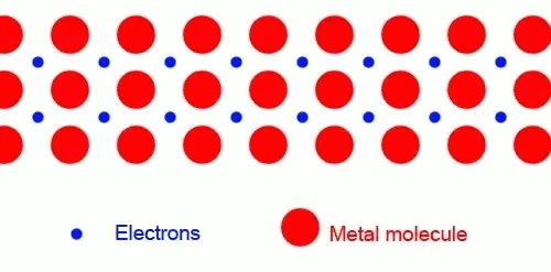
Figure 1. Electromigration in metal interconnects (left), atomic-level illustration (right) [5]
The dimensions of today's modern electronic components have been reduced to such an extent that even solder joints can develop a critical current density that can cause electromigration. For components used in surface mount technology (components are soldered to a solder joint, as opposed to classical through holes), the phenomenon is most often investigated in the case of ball grid array (BGA) or 3D-IC [6], due to the small size of the solder joints. A novel feature of my research is that I performed my studies on passive chip-sized surface mount components. The parts investigated are 1.6 x 0.8 mm (size code 0603) and 1 mm x 0.5 mm (size code 0402) in size which are worth addressing, as these and even smaller parts are already used in high-reliability applications (e.g., automotive, aerospace) [7].
The research goals, open questions
In my research, I seek to answer the question of the effect of long-term current loading on the microstructure and reliability in lead-free tin-silver-copper (Sn-3Ag-0.5Cu) solder joints of passive chip-sized components. A critical parameter for the mechanical properties of soldered joints is the thickness of the intermetallic layer that forms between the solid solder joint and the soldering surfaces during reflow soldering. The current load and the associated increased thermal load have a significant effect on the change in layer thickness, potentially reducing the mechanical strength of the joint [8].
Methods
For the experiments, I designed a circuit with 90° and 135° wire connection angles (Figure 2, B), because the simulation studies of our research group showed that the current density is highest in these cases (Figure 2, A). During the investigation, I tested hundreds of surface-mounted 0 Ω components (0603 and 0402 size codes) on ceramic-based substrates. The components were divided into three groups and compared: DC load, isothermally aged (to deconvolute the effect of elevated temperature), and unloaded post-soldering reference samples. The applied load time extended to 4000 h with 2A (0402) and 2.5 A current load (0603), respectively. The current load was applied at an ambient temperature of 40°C and the isothermal aging at 120°C (the currently loaded parts were heated to 110°C and 130°C, respectively).
Microstructural analysis of the joints was carried out on cross-sectional samples. This requires the circuit boards to be sectioned, embedded in epoxy, and then polished following a wet grinding process. The samples were examined by optical microscopy, scanning electron microscopy (SEM), and energy-dispersive X-ray spectroscopy (EDX). Selective electrochemical etching was used to remove the tin from the solder joint, revealing the fine structures of the intermetallic compounds. The intermetallic layer thickness distribution was determined from optical microscopy images by image processing. The mechanical properties of the soldered joints were analyzed by shear testing, where the test equipment uses a shear-direction knife to shear off the parts and examined the required force curve.
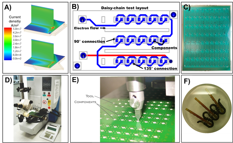
Figure 2. High-current-density cluster points based on simulation results (A), designed test circuit with 90° and 135° wire connection angles (B), fabricated circuits (C). Shear strength test rig (D), shear strength test (E), cross-sectional grinding of 15 epoxy embedded parts (F) [9]
Results
After 4000 hours of current loading, the solder joint has degraded significantly. A large intermetallic alloy of Cu6Sn5 composition is visible along the component metallization. The source of the copper in this is the solder joint where the copper layer has thinned. The following figure shows that microvoids were formed along the intermetallic layer and its thickness remained limited due to electromigration. The diffusion-inhibiting effect of the plate-like Ag3Sn was also observed (Figure 3, C).
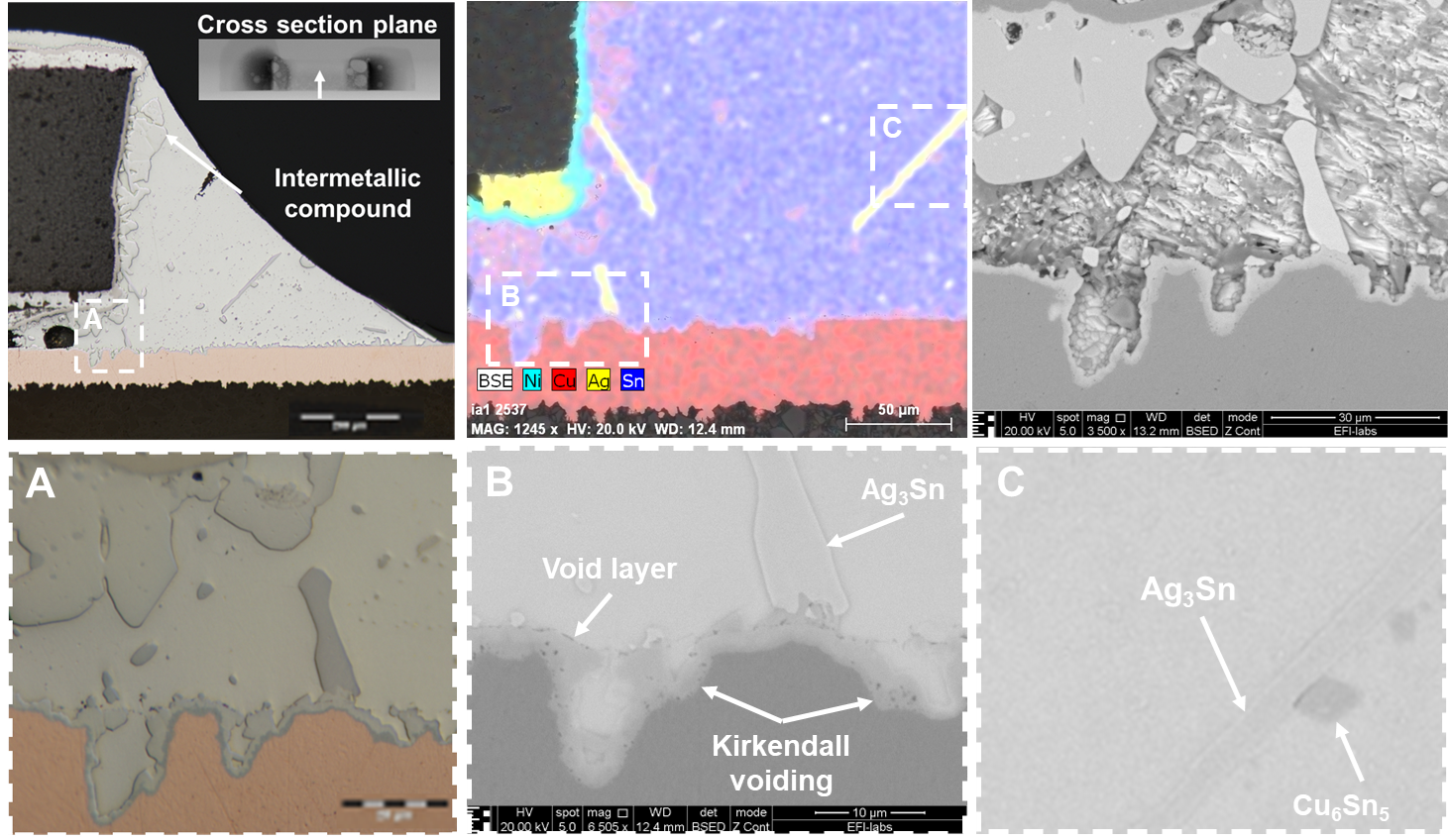
Figure 3. Optical micrograph (left), scanning electron micrograph (middle, right) after 4000 hours of current loading for part 0402
Quantitative analysis showed an asymmetric increase in the intermetallic layer as a function of the current direction (anode and cathode side) in the current-loaded samples (Figure 4, blue), which is approximately double compared to the reference (green), with a similar increase in the heat-loaded samples (orange).
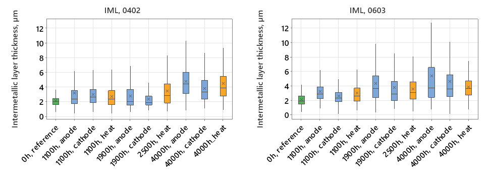
Figure 4. Distribution of intermetallic layer thickness at different loading times.
Thickening of the intermetallic layer can lead to a deterioration of the mechanical properties of the soldered joint. The latter was confirmed in the shear strength test: after 4000 hours of exposure, the shear strength of solder joints decreased by about 24% for 0603 parts, with a higher standard deviation for the current stressed samples (Figure 5).
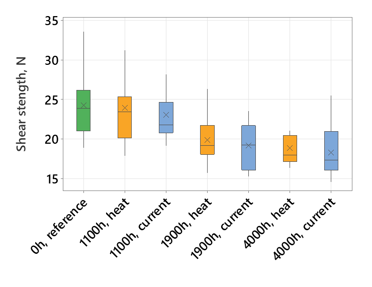
Figure 5. Shear strength of soldered joints (green: reference, blue: current loaded, orange: heat loaded) after different loading times
When examining the fracture surfaces, the currently loaded samples showed brittle Cu6Sn5 alloy, which can be attributed to thickening along the component metallization due to electromigration.
Expected impact and further research
The research has shown that even for passive chip-sized components, the current load on the component should be considered. By applying the presented methods, it is possible to investigate different novel composite solder materials (e.g., ceramic nanoparticle doped), as their exposure to electromigration may vary. The latest results covering the extended 4000-hour testing period are under submission to an international peer-reviewed journal (D1/Q1 level).
Publications
International, peer-reviewed journal papers, written in the English language
[L1] Geczy, A., Straubinger, D., Kovacs, A., Krammer, O., Mach, P. and Harsányi, G. (2018), "Effects of high current density on lead-free solder joints of chip-size passive SMD components", Soldering & Surface Mount Technology, Vol. 30 No. 2, pp. 74–80., doi: 10.1108/SSMT-10-2017-0032.
[L2] Straubinger, D., Géczy, A., Sipos, A., Kiss, A., Gyarmati, D., Krammer, O., Rigler, D., Bušek, D. and Harsányi, G. (2019), "Advances on high current load effects on lead-free solder joints of SMD chip-size components and BGAs", Circuit World, Vol. 45 No. 1, pp. 37–44., DOI: 10.1108/CW-11-2018-0088.
International, peer-reviewed conference papers, written in the English language
[R1] Géczy, A., Straubinger, D., Hurtony, T., Krammer, O., & Kovács, A. (2017). Investigating current density in the lead-free solder joints of surface mounted resistors with experimental approach. In 2017 40th International Spring Seminar on Electronics Technology (ISSE) (pp. 1–6). IEEE., doi: 10.1109/ISSE.2017.8000930.
[R2] Straubinger, D., Rigler, D., Géczy, A., & Synkiewicz-Musialska, B. (2020). Electromigration in lead-free solder joints on ceramic PCB substrates. In 2020 IEEE 26th International Symposium for Design and Technology in Electronic Packaging (SIITME) (pp. 52–56). IEEE., doi: 10.1109/SIITME50350.2020.9292158
[R3] Straubinger, D., & Géczy, A. (2021). Effect of highly increased current density in the microstructure of lead-free solder joints. In 2021 23rd European Microelectronics and Packaging Conference & Exhibition (EMPC) (pp. 1–5). IEEE.,
doi: 10.23919/EMPC53418.2021.9584980
Submitted, but not yet reviewed journal papers:
Straubinger D., Hurtony T., Géczy A. (2022). Impact of electromigration and isothermal ageing on lead-free solder joints of chip-sized SMD components, preprint available
Links
BME ETT online interactive laboratory
References
[1] Kumar, A., Yang, Y., Wong, C. C., Kripesh, V., & Chen, Z. (2008). Effect of Electromigration on the Mechanical Performance of Sn-3.5Ag Solder Joints with Ni and Ni-P Metallizations. Journal of Electronic Materials 2008 38:1, 38(1), 78–87. https://doi.org/10.1007/S11664-008-0565-6
[2] Li, X., Sun, F., Liu, Y., Zhang, H., & Xin, T. (2014). Geometrical size effect on the interface diffusion of micro solder joint in electro-thermal coupling aging. Journal of Materials Science: Materials in Electronics, 25(9), 3742–3746. https://doi.org/10.1007/S10854-014-2084-Y
[3] Black, J. R. (1969). Electromigration—A brief survey and some recent results. IEEE Transactions on Electron Devices, 16(4), 338–347.
[4] Blech, I. A. (1976). Electromigration in thin aluminum films on titanium nitride. Journal of applied physics, 47(4), 1203-1208., https://doi.org/10.1063/1.322842
[5] Electromigration - Terris’s Blog. (n.d.). Accessed at: 2022.06.24,: https://terris.wordpress.com/portfolio/electromigration/
[6] Ho, C. E., Lee, P. T., Chen, C. N., & Yang, C. H. (2016). Electromigration in 3D-IC scale Cu/Sn/Cu solder joints. Journal of Alloys and Compounds, 676, 361–368.
[7] Tao, Y., Ding, D., Li, T., Guo, J. and Fan, G. (2017), “Reflow of tiny 01005 capacitor/SAC305 solder joints in protective atmosphere”, Soldering & Surface Mount Technology, Vol. 29 No. 3, pp. 144–150.
[8] Wang, X. J., Zeng, Q. L., Zhu, Q. S., Wang, Z. G., & Shang, J. K. (2010). Effects of Current Stressing on Shear Properties of Sn-3.8Ag-0.7Cu Solder Joints. Journal of Materials Science & Technology, 26(8), 737–742. https://doi.org/10.1016/S1005-0302(10)60116-8
[9] Website of the Department of Electronics Technology, BME. (n.d.). Accessed at: 2022.06.24., https://www.ett.bme.hu/laborok/assembly/shear_test