|
|
BMe Research Grant |
|

Török Tímea Nóra
BMe Research Grant - 2023
Ist Prize
![]()
Doctoral School of Physics
BME TTK, Department of Physics
Supervisor: Dr. Halbritter András
Experimental study and neuromorphic applications of memristors
Introducing the research area
The focus of my research is the development of nanometer-scale resistive switching memory devices and the study of their physical processes. I also aim to create neuromorphic, signal processing networks utilizing these devices.
Brief introduction of the research place
To develop memristors, the nanofabrication infrastructure located at the Nanosensors Laboratory at the Institute of Technical Physics and Materials Science, Centre for Energy Research is essential. Custom-built measurement setups developed by the Atomic and Molecular Electronics Group at the Department of Physics, BME are also of vital importance. The He liquefier facility at the University provides a unique opportunity for low-temperature studies of memristors.
History and context of the research
Resistive switching memories – or memristors – are generally metal-insulator-metal nanostructures whose conductance can be changed by electrical signals applied to their electrodes, thereby storing information in the conductance [1]. During resistive switching, a conductive channel (filament) of a nanometer-scale – in some cases even atomic-scale [O1] – diameter is formed in the active region, which can be complemented with various physical mechanisms, depending on the material structure of the memristor [2] (Figure 1). Utilizing the voltage- and time-dependent dynamics of the non-volatile types of resistive switching, multi-level (analog) programming can also be implemented (Figure 1.a) [O1,O3-O5,S1]. These resistive switching memories provide a promising platform for hardware-level encoding of large synaptic weight matrices in artificial neural networks [3-4]. Other types of memristors have volatile memory (Figure 1.b) [O2] and can be used for artificial neural signal generation tasks [5]. Exploiting the switching dynamics of various memristors, hardware-level signal recognition and processing tasks can be implemented using only a few devices [S2-S3]. Thanks to the tuneable noise characteristics of memristors [O6], they can be suitable for the hardware implementation of stochastic optimization algorithms [6,S4]. Combining their computational and long-term memory capabilities – overcoming the limitations of von Neumann architectures – resistive switching memories represent a promising direction of future development in the field of new information technologies [7].
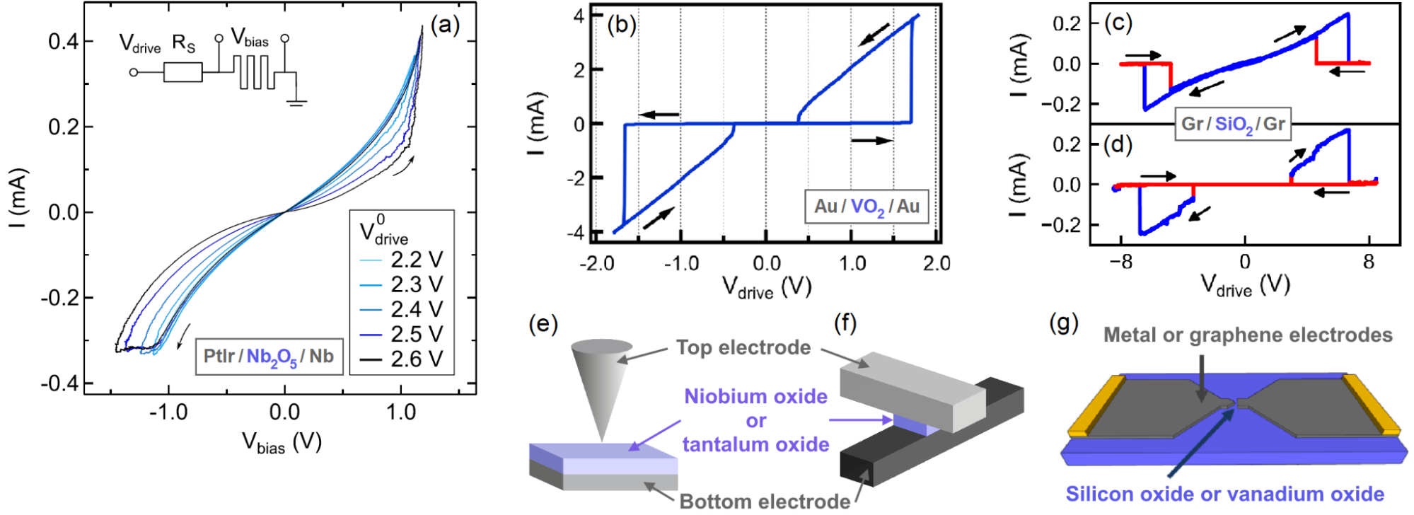
Figure 1: (a-d) Current-voltage characteristics and (e-g) schematics of typical structures of different memristors. [O1-O4]
The research goals, open questions
One objective of my research is to explore and model the physical processes in various resistive switching memories. Another important endeavor is to develop on-chip devices suitable for signal processing, utilizing the internal mechanisms of the devices.
Size and scalability of the active region are critical properties from a technological point of view, but the discovery of the unique structure of the nanofilaments and their in-situ, non-destructive experimental investigation is a challenging task. It is possible to image the filaments with electron microscopy methods [8,9], but studying the operation of a vertical memristor (Figure 1.e-f) with those techniques is limited. Therefore, I adapted a superconducting spectroscopy method for studying Nb2O5 and Ta2O5-based memristors, which has been widely used earlier to map the quantum transport properties of pure atomic wires [10].
The operation of memristors is inherently stochastic in nature, which is manifested through several measurable physical quantities of the devices. Such stochastic values are the resistance states and set times experienced during periodically cycled measurements. The correlations of these quantities and the distribution of the set times provide valuable information on the underlying switching mechanism. My goal is to study the operation of SiO2-based resistive switching memories through these quantities, focusing on the applicability of nucleation theory [11].
Methods
Sample fabrication
At the beginning of my studies, I mainly focused on studying point-contact junctions, which I created in an STM (scanning tunneling microscope) arrangement using a sharp tip on top of a thin layer made of resistive switching material (Nb2O5 or Ta2O5) (Figure 1.e). The advantage of this technique is the ability to create new junctions by repeatedly lifting the tip and contacting it at another location. For these experiments, I created resistive switching thin layers on the surface of carrier metal layers by anodic oxidation [O1,O5-O6]. One disadvantage of the STM point-contact technique is that contacts are short-lived, being stable only at the ~10-minute time scale of the STM system. Another limitation is that these point-contact samples cannot be integrated. Therefore, an important goal was the development of on-chip memristors that meet technological requirements in terms of scalability. I have participated in the production and optimization of such on-chip memristors by electron beam lithography (EBL) during the last years [O2-O3,O6]. I learned the techniques of EBL and thin film deposition at the Nanosensors Laboratory with the help of Dr László Pósa.
Superconducting spectroscopy
The conductance of an atomic wire can be expressed by the
Landauer
formula,
![]() ,
where
,
where
![]() i
is the electron transport probability in the i. channel, M is
the number of conduction channels and G0 = 2e2/h
is the conductance quantum. Superconducting subgap spectroscopy is a direct
method for the experimental determination of the
i
is the electron transport probability in the i. channel, M is
the number of conduction channels and G0 = 2e2/h
is the conductance quantum. Superconducting subgap spectroscopy is a direct
method for the experimental determination of the
![]() i
transmission eigenvalues, the essence of which is fitting the current-voltage
characteristics measured in the range of the superconducting energy gap [12].
Using this method, I demonstrated that filaments with a diameter of only one
atom can be formed in Nb2O5 memristors [O1]. In the case
of more conductive transition metal junctions that already consist of 2 – 3
atoms, 10 – 15 conduction channels are realistic due to the presence of many
valence electrons [10]. These diffusive nanowires can be well modeled with a
universal transmission distribution derived from calculations using random
matrix theory [13]. Based on the work of Yu. V. Nazarov, the presence of an
extensive defect (barrier) affects the transmission distribution, which can be
accurately modeled as a function of the parameter
i
transmission eigenvalues, the essence of which is fitting the current-voltage
characteristics measured in the range of the superconducting energy gap [12].
Using this method, I demonstrated that filaments with a diameter of only one
atom can be formed in Nb2O5 memristors [O1]. In the case
of more conductive transition metal junctions that already consist of 2 – 3
atoms, 10 – 15 conduction channels are realistic due to the presence of many
valence electrons [10]. These diffusive nanowires can be well modeled with a
universal transmission distribution derived from calculations using random
matrix theory [13]. Based on the work of Yu. V. Nazarov, the presence of an
extensive defect (barrier) affects the transmission distribution, which can be
accurately modeled as a function of the parameter
![]() =
Rwire/Rbarrier [14], which can be applied
to Ta2O5-based memristors [O4].
=
Rwire/Rbarrier [14], which can be applied
to Ta2O5-based memristors [O4].
Results
Superconducting spectroscopy on Nb2O5 and Ta2O5 memristors
In
search for the ultimate smallest active region that can be created in
resistive switching memories, I first examined point-contact memristors based
on Nb2O5 (Figure 2.a). Stopping at the different states
of the switching curve (Fig. 2b) and measuring low-signal (~10 mV) subgap
characteristics, I proved that a single dominant channel (![]() )
forms in the ON states around G0 (Fig. 2.c). These
measurements were the first to demonstrate the presence of truly single-atom
filaments in transition metal oxide memristors [O1].
)
forms in the ON states around G0 (Fig. 2.c). These
measurements were the first to demonstrate the presence of truly single-atom
filaments in transition metal oxide memristors [O1].
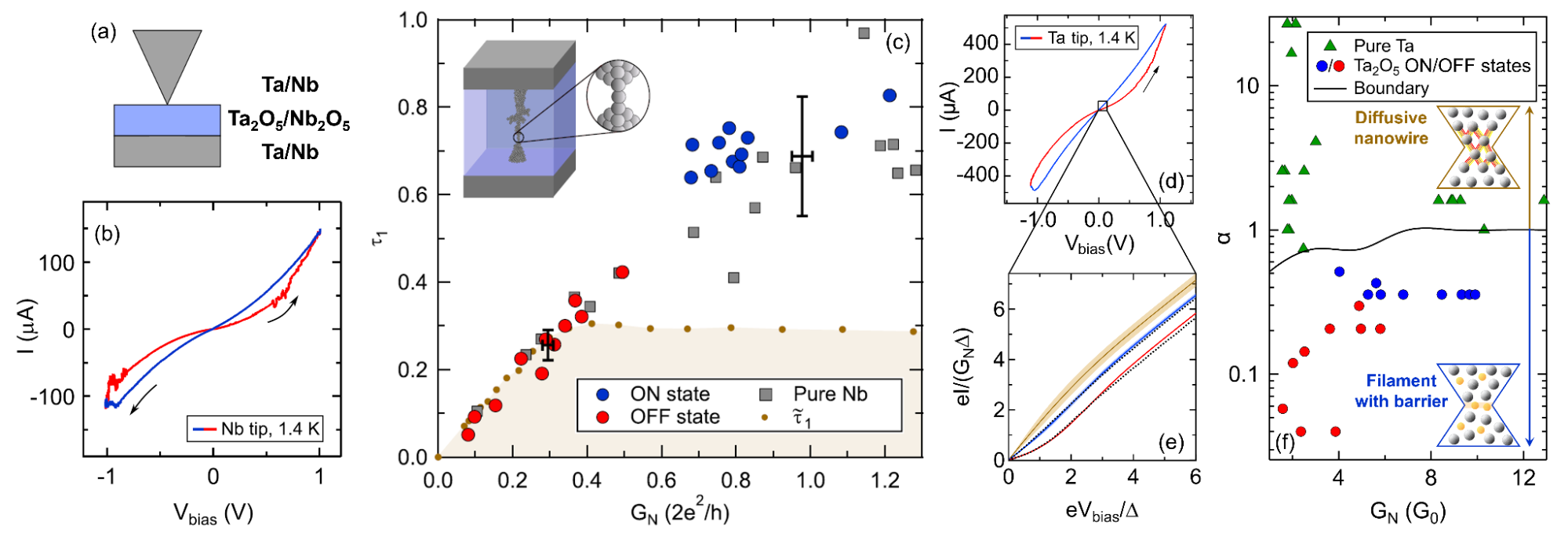
Figure 2:
(a) Scheme of an STM point-contact. (b) Resistive switching at a temperature
of 1.4 K on a Nb/Nb2O5/Nb contact. (c) Transmission of
the first conduction channel indicates atomic contact in the ON states around
G0. (d) Resistive switching and (e) subgap characteristics at a
temperature of 1.4 K on a Ta/Ta2O5/Ta contact. (f) The
![]() parameter
of the extended defect as a function of conductance; illustration of models
corresponding to the value of
parameter
of the extended defect as a function of conductance; illustration of models
corresponding to the value of
![]() on
both sides of the boundary [O1,O4].
on
both sides of the boundary [O1,O4].
I
extended my studies to Ta2O5-based memristors (Figure
2.d) operated in a higher conductance range (2 – 10 G0).
Here, it is necessary to model the contact with transmission distributions to
properly fit the subgap characteristics (Figure 2.e). In the ON/OFF states
(blue/red curve in Fig. 2.e), I discovered differences compared to the pure,
diffusive nanowire model (brown curve in Fig. 2.e). In all memristor states,
an extensive defect limits the transport in the filament, which can be deduced
from the
![]() ON,OFF
<
1 tendency obtained from the fits (Figure 2.f) [O4].
ON,OFF
<
1 tendency obtained from the fits (Figure 2.f) [O4].
Stochastic nucleation in SiO2 memristors
By the statistical analysis of the set time distribution of SiO2-based nanogap memristors (Fig. 3a-b) [15], I revealed that the set operation can be described as a nucleation process [O3]. The essence of the model is the nucleation energy that varies randomly per cycle, with a correlation parameter of 200 switching cycles. The histogram of series longer than that parameter shows a lognormal distribution (Figure 3.d), while that of shorter series shows an exponential distribution (Figure 3.e).
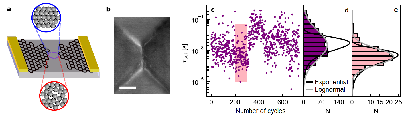
Figure 3: (a) Scheme of a Gr/SiO2/Gr nanogap sample and illustration of its crystalline/amorphous structure in the ON/OFF states. (b) Scanning electron micrograph of the active region, scale bar: 200 nm. (c) Evolution of the set time in Gr/SiO2/Gr memristors. Histograms of (d) the entire data set and (e) a short part of the data [S1,O3].
Memristor-based neuromorphic circuits
A Ta2O5 memristor biased at a small signal level can recognize patterns hidden in a noisy environment because a short/long spike at its input causes a short-term/permanent resistance change. Complementing the circuit with a self-made VO2 memristor-based oscillator, an autonomous neural spike detector/transmitter unit can be realized (Figure 4.a) [S2,O7]. By connecting a similar oscillator unit to the output of a piezoelectric cantilever (Figure 4.b), an artificial auditory sensor unit can be established that shows characteristics similar to natural hearing [S3].
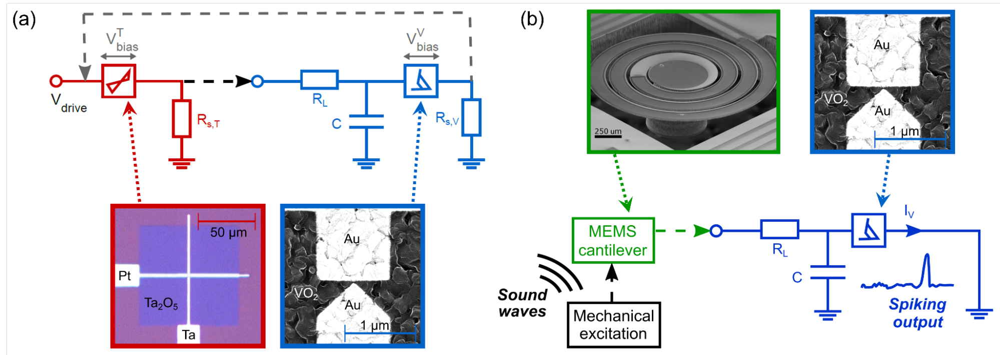
Figure 4: (a) Neural spike detector/transmitter unit from Ta2O5 and VO2 memristors. [S2,O7] (b) Concept of an artificial auditory sensor unit by connecting a piezoelectric cantilever [16] and a VO2 memristor [S3].
Expected impact and further research
In the future, the device-level application of the dynamical properties of memristors will receive a lot of emphasis, through publications (e.g. [O7]) based on the works [S2] and [S3]. In addition, our goal is to develop ultrafast (fosc. > 10 MHz), VO2-based oscillators [17,18]. Another objective is to utilize the tuneable noise characteristics of memristors [O6], by implementing stochastic optimization procedures at the hardware level [S4,19].
Publications, references, links
List of corresponding own publications.
[O1] Tímea Nóra Török, Miklós Csontos, Péter Makk, András Halbritter. Breaking the Quantum PIN Code of Atomic Synapses. Nano Letters 20, 1192–1200 (2020)
[O2] László Pósa, Péter Hornung, Tímea Nóra Török, Sebastian Werner Schmid, Sadaf Arjmandabasi, György Molnár, Zsófia Baji, Goran Dražić, András Halbritter, János Volk. Interplay of Thermal and Electronic Effects in the Mott Transition of Nanosized VO2 Phase Change Memory Devices. ACS Applied Nano Materials 6, 9137–9147 (2023)
[O3] Tímea Nóra Török, János Gergő Fehérvári, Gábor Mészáros, László Pósa, András Halbritter. Tunable, Nucleation-Driven Stochasticity in Nanoscale Silicon Oxide Resistive Switching Memory Devices. ACS Applied Nano Materials 5, 6691–6698 (2022)
[O4] Tímea Nóra Török, Péter Makk, Zoltán Balogh, Miklós Csontos, András
Halbritter. Quantum Transport Properties of Nanosized Ta2O5
Resistive Switches: Variable Transmission Atomic Synapses for Neuromorphic
Electronics.
https://pubs.acs.org/doi/10.1021/acsanm.3c04769
(2023)
[O5] Dániel Molnár, Tímea Nóra Török, Botond Sánta, Agnes Gubicza, András Magyarkuti, Roland Hauert, Gábor Kiss, András Halbritter, Miklós Csontos In situ impedance matching in Nb/Nb2O5/PtIr memristive nanojunctions for ultra-fast neuromorphic operation. Nanoscale 10, 19290–19296 (2018)
[O6] Botond Sánta, Zoltán Balogh, László Pósa, Dávid Krisztián, Tímea Nóra Török, Dániel Molnár, Csaba Sinkó, Roland Hauert, Miklós Csontos, András Halbritter. Noise Tailoring in Memristive Filaments. ACS Applied Materials & Interfaces 13, 7453–7460 (2021)
[O7] Dániel Molnár, Tímea Nóra Török, Roland Kövecs, László Pósa, Péter Balázs, Zoltán Balogh, György Molnár, Nadia Jimenez Olalla, Juerg Leuthold, János Volk, Miklós Csontos, András Halbritter. Autonomous neural information processing by a dynamical memristor circuit. Available: https://arxiv.org/abs/2307.13320
Supervisory activity.
[S1] János Gergő Fehérvári. Experimental study of time scales in nanoscale phase change memories. TDK thesis (2020)
[S2] Antal Roland Kövecs. Realization of a memristor-based detector circuit with neurodynamical behavior. TDK thesis (2022)
[S3] Antal Roland Kövecs. Designing a memristor-based signal processing unit for cochlear implants. BSc thesis (2023)
[S4] János Gergő Fehérvári. Stochastic phenomena in resistive switching memories. BSc thesis (2021)
Table of links.
Electron transport in nanowires
International Roadmap for Devices and Systems (IRDS™) 2022 Edition
List of patents related to memristors
List of references.
[1] M. A. Zidan et al. The future of electronics based on memristive systems. Nature Electronics 1, 22–29 (2018)
[2] Z. Wang et al. Resistive switching materials for information processing. Nature Reviews Materials 5, 173–195 (2020)
[3] S. Ambrogio et al. Equivalent-accuracy accelerated neural-network training using analogue memory. Nature 558, 60–67 (2018)
[4] Q. Xia, J. J. Yang. Memristive crossbar arrays for brain-inspired computing. Nature Materials 18, 309–323 (2019)
[5] W. Yi et al. Biological plausibility and stochasticity in scalable VO2 active memristor neurons Nature Communications 9, 4661 (2018)
[6] F. Cai et al. Power-efficient combinatorial optimization using intrinsic noise in memristor Hopfield neural networks. Nature Electronics 3, 409–418 (2020)
[7] International Roadmap for Devices and Systems (IRDS™), 2022 Edition: Beyond CMOS and Emerging Materials Integration
[8] Y. Yang et al. Observation of conducting filament growth in nanoscale resistive memories. Nature Communications 3, 732 (2012)
[9] D.-H. Kwon et al. Atomic structure of conducting nanofilaments in TiO2 resistive switching memory. Nature Nanotechnology 5, 148–153 (2010)
[10] E. Scheer et al. The signature of chemical valence in the electrical conduction through a single atom contact. Nature 394, 154 (1998)
[11] V. G. Karpov et al. Field-induced nucleation in phase change memory. Phys. Rev. B 78, 052201 (2008)
[12] N. Agrait et al. Quantum properties of atomic-sized conductors. Physics Reports 377, 81 (2003).
[13] C. W. J. Beenakker. Random-matrix theory of quantum transport. Reviews of Modern Physics 69, 731–808 (1997)
[14] Yu. V. Nazarov. Limits of universality in disordered conductors. Phys. Rev. Lett. 73, 134–137 (1994)
[15] L. Pósa et al. Multiple Physical Time Scales and Dead Time Rule in Few-Nanometers Sized Graphene-SiOx-Graphene Memristors. Nano Letters 17, 11, 6783–6789 (2017)
[16] P. Udvardi et al. Spiral-Shaped Piezoelectric MEMS Cantilever Array for Fully Implantable Hearing Systems. Micromachines 8, 311 (2017)
[17] Md. Suruz Mian et al. Self-oscillation up to 9 MHz based on voltage triggered switching in VO2/TiN point contact junctions. Journal of Applied Physics 117, 215305 (2015)
[18] B. Zhao et al. Low-Power Microwave Relaxation Oscillators Based on Phase-Change Oxides for Neuromorphic Computing. Physical Review Applied 11, 014020 (2019)
[19] János Gergő Fehérvári. Stochastic Optimisation using Memristor-based Tunable Noise Contribution. TDK thesis (2022)