 |
BMe Research Grant |

|


Doctoral School of Physical Sciences
Department of Physics/Institute of Physics
Supervisor: Dr. György Mihály
Superconductivity-based nanoelectronics
Introducing the research area
I study the electronic transport in point contacts between a superconductor and a normal metal. Using our custom built measurement system, I can probe various fundamental material parameters such as the degree of ferromagnetism on the scale of a few nanometers. During my research work I have investigated a variety of physical systems, including dilute magnetic semiconductors, layered metallic structures, and resistive switching materials.
Brief introduction of the research place
My research work is conducted at the Solid State Physics Laboratory at the Department of Physics, where the main research fields are nanophysics and quantum transport. The laboratory is well-equipped for low temperature transport measurements.
History and context of the research
 The
concept of spintronics, i.e. the spin based electronics is based on the
two quantized levels of the spin of an electron in any given direction [1]. This property allows direct representation of digital data, however, efficient manipulation and readout of the spin state raise
fundamental questions in terms of material parameters and method of integration into
semiconductor devices [2]. As the typical size of the proposed spintronic
devices falls in the range of 10 nm, efficient local probing methods have to be
used to gain information on the spin states.
The
concept of spintronics, i.e. the spin based electronics is based on the
two quantized levels of the spin of an electron in any given direction [1]. This property allows direct representation of digital data, however, efficient manipulation and readout of the spin state raise
fundamental questions in terms of material parameters and method of integration into
semiconductor devices [2]. As the typical size of the proposed spintronic
devices falls in the range of 10 nm, efficient local probing methods have to be
used to gain information on the spin states.
Unlike magnetic data storage, the field of resistive switching memories based on a novel passive circuit element, the memristor is relatively young [3]. Resistive memory cells contain an electrochemically active region whose resistance can be altered by applying a bias voltage on the device. Its favorable properties, such as high speed, long retention time and high endurance make such systems a viable next generation solid state memory candidate [4], referred to as RRAM.
The research goal, open questions
Spintronics
 |
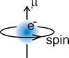
| Left: The
charge conversion process called Andreev reflection transfers two charge
quanta through the SN interface as a hole is reflected back instead of the
incoming electron. Right: Experimental data on different materials
exhibiting spin polarization between 0 for Cu and almost 100% for
CrO2 (published by Soulen et al [6]). |
The presence of the Cooper pair condensate in a
superconductor leads to new phenomena in the electronic transport through a
superconductor-metal interface [5]. As the Cooper pairs form spin singlet, the transport is
sensitive to the magnetic ordering in normal metal, which offer an effective
method for locally probing ferromagnetism. The point contact Andreev
reflection (PCAR) technique based on this property was developed by Soulen's team in 1998 [6] and has been extensively used ever since. Despite the
simple and elegant theoretical approach, experimental realization raised
many questions. One of the main objectives of my PhD work is to systematically investigate the
proper parameters for such measurements in terms of the junction diameter and
material parameters.
The resistive switching effect
 |
|
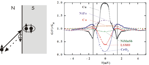
Left: The solid state electrochemical cycle resulting in the formation and retraction of Ag filaments inside the Ag2S matrix. Right: The schematic view of the atomic switch published by the group of Terabe [9]. |
The application of resistive switching effect to
memory cells and novel computer architectures requires the profound understanding of
the details of underlying electrochemical processes [7]. The fundamental picture of the formation and retraction of
conducting filaments resulting in the change of the transmission of junction
can be investigated using point contact Andreev reflection spectroscopy. It is
important to note that this method effectively probes the properties of the
junction in situ with no external probing or subsequent disassembly of the
junction being necessary. This unique property provides a novel tool that
contributes to the understanding of memristive systems down to the single atomic
scale where quantization effects are expected to emerge in the conductance [8]. The concept of single atomic memory, first envisioned
by the group of Terabe [9], is an exciting outlook with a theoretical maximum of data
density of 10 TB/inch2.
Methodology
Experimental
 |
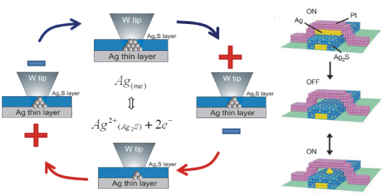
| Left: The drawing of the
sample holder head exhibiting a twofold actuation
system. Right: Zoom in to the apex of the tip. |
The controllable formation of nanoscale metallic junctions between a sample and a tip of different materials required a novel measurement system, developed and subsequently upgraded during my diploma and PhD work on the basis of the earlier work [10] of András Halbritter and Szabolcs Csonka.
The two stage actuation system of the sample holder provides the capability of fine tuning of the junction diameter down to the single atomic scale, yet the coarse movement of the tip is in the range of a few millimeters. The self-developed modular measurement program based on National Instrument’s Measurement Studio suite provides great flexibility of measurement design and makes the investigation of various, radically different physical systems possible.
For low temperature measurements care must be taken of noise filtering and of ensuring proper thermalization of the wiring of the sample holder. In our system, this goal was achieved by a sophisticated electronic design, reaching an estimated 50μVrms noise floor.
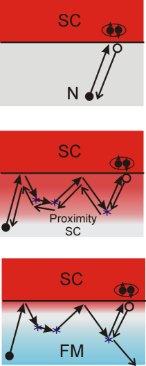 |
|
Top: A single Andreev reflection process. Middle: Multiple scatterings near the SN interface. Note that the reflected hole traverses back on the exact same pathway resulting in strong electron-hole pairing in the N side, i.e. proximity superconductivity. Bottom: in a ferromagnetic material no proximity superconductivity occurs due to fast decoherence. |
Theory
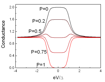 |
| Differential conductance curves for SN
junctions with the spin polarization ranging from 0 to 100% on the normal
metal side. |
On a superconductor-normal metal (SN) interface, a new type of charge transport, the Andreev reflection emerges, effectively resulting in the simultaneous transmission of double electronic charges with opposite spin states. In ferromagnetic metals, however, the spin ordering suppresses this process, and the resulting conductance curve depends on the degree of the charge carrier spin polarization (P) in the normal metallic side of the junction. Andreev reflection is also suppressed for low transparency (tunnel) junctions, reducing the subgap conductance of the junction.
The coherent nature of mesoscopic transport results in additional phenomena for slightly larger junctions in the diffusive limit. Multiple scatterings inside the junction area bring about interference effects observable in the conductance of the point contact. An important consequence of the diffusive transport through a SN interface is the appearance of superconducting pair correlations in the normal metal providing the microscopic origin of proximity superconductivity. This effect, however, vanishes for ferromagnetic materials due to the fast decoherence of the electron-hole pair in different spin subbands.
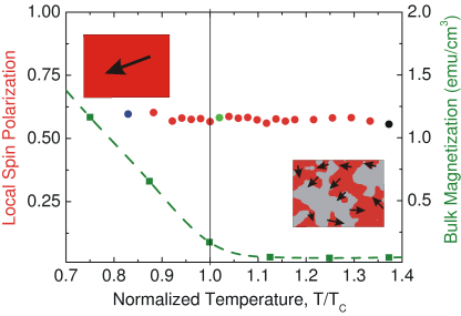 |
|
Local spin polarization in the dilute magnetic semiconductor (In,Mn)Sb measured by PCAR as a function of the temperature on the nanometer scale. The insets show the scheme of the expected local magnetic ordering below and above the Curie temperature. |
Results
Dilute magnetic semiconductors
III-V semiconductors doped with a few percent of Mn have recently been considered as a pathway to integrate spintronic devices with present semiconductor-based electronics. I have investigated (In,Mn)Sb exhibiting a Curie temperature of Tc=5.4K. This low transition temperature has provided the possibility to investigate the magnetic phase transition using Nb as a superconducting counterelectrode. I have found a high degree of spin ordering (approx. 60%) at low temperatures. Compared to the results of bulk characterization methods, such as SQUID, I have found that local ferromagnetic ordering does not disappear at Tc, even though the sample does not exhibit macroscopic ordering. This striking difference is attributed to the percolating nature of the magnetic phase transition in this material, with small magnetically ordered islands existing far above the Curie temperature [G1].
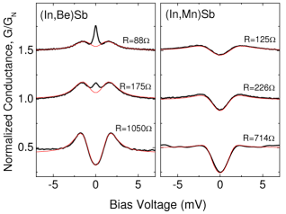 |
|
The evolution of the zero bias conductance peak in (In,Be)Sb. Note that this feature is completely missing in the (In,Mn)Sb sample due to the ferromagnetic ordering. |
Size effects and proximity superconductivity
The unique stability of the measurement system enabled us to systematically investigate size effects of the electronic transport in SN junctions. Based on my measurements on (In,Mn)Sb I have shown that for junctions in the diffusive limit, there is a systematic deviation from the theory. Consequently, for the reliable determination of spin polarization, junctions in the ballistic limit have to be measured. Further investigations on the non-magnetic sample (In,Be)Sb of similar charge carrier concentration showed the presence of zero bias anomalies attributed to the mesoscopic interference effects explained above. In contrast, for (In,Mn)Sb, phase coherence is destroyed by the ferromagnetic ordering, which explain the different characteristics of the two samples [G3].
Spin diffusion length in metals
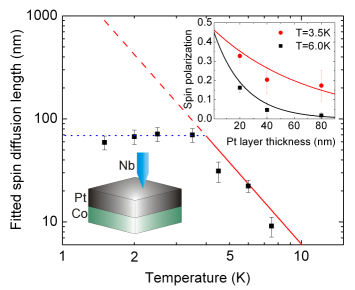 |
|
The temperature dependence of the spin diffusion length in Pt. Bottom inset shows the measurement geometry. Upper inset demonstrates the exponential decay of the spin polarization at a given temperature. |
The persistence of an injected spin state in paramagnetic metals is determined by the spin lifetime, which is an important material parameter effectively determining the size of spintronic devices, such as GMR sensors. I have investigated the decay of the spin polarization in paramagnetic metals (PM) evaporated on the top of a thick ferromagnetic layer. By varying the PM layer thickness, I have determined the spin diffusion length, as the characteristic length scale from the exponential dependence of spin polarization. In Pt, I have shown that the temperature dependence of the spin diffusion length is consistent with the power law behavior of the Elliott – Yafett model [G5].
Memristive systems
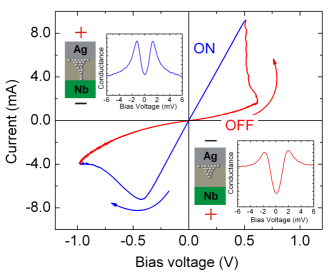
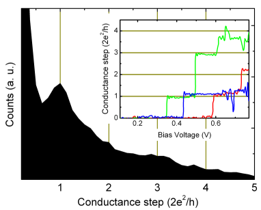
I have investigated thin Ag2S layers on Ag exhibiting resistive switching due to the formation and distraction of metallic silver filaments through the semiconducting surface layer. I have demonstrated that the Andreev reflection measurements show the expected change of transmission between the low resistance (ON) and high resistance (OFF) state which provides a direct proof of the scheme explained above. When the junction diameter is comparable to the size of a single silver atom, quantized conductance steps can be observed that prove to agree with 2e2/h, the conductance value of a single Ag atom [G4, G6].
 |
 |
|
Left: I-V characteristics of a Ag-Ag2S-Nb
resistive switch. Andreev reflection measurements (inset) provide a direct
proof of the scheme of the formation of metallic silver filaments in the
Ag2S layer resulting in more than one order of change of the
zero bias resistance. Right: The histogram of the quantized conductance steps for small junctions in the few atomic regime exhibiting a peak around 2e2/h which is the conductance of a single Ag atom. Inset shows individual traces. |
Expected impact and further research
During my PhD work I have demonstrated the application of superconductivity as a probe on many novel systems ranging from spintronic applications to the resistive switching effect. The results have been published in leading international peer-reviewed journals of the field.
Further experiments will be performed on other materials exhibiting exotic magnetic ordering as well as magnetic memory effects. Instrumental upgrades will provide further flexibility in terms of experimental parameters, such as high speed measurements and scanning probe functionality.
Publications, references, links
Publications
[G1] A. Geresdi, A. Halbritter, M. Csontos, S. Csonka, G. Mihály, T. Wojtowicz, X. Liu, B. Janko, J. K. Furdyna. Nanoscale spin polarization in the dilute magnetic semiconductor (In,Mn)Sb
Phys. Rev. B 77, 233304 (2008)
[G2] L. Hofstetter, A. Geresdi, M. Aagesen, J. Nygård,
C. Schönenberger, S. Csonka. Ferromagnetic Proximity Effect in a
Ferromagnet–Quantum-Dot–Superconductor Device
Phys. Rev. Letters
104, 246804 (2010)
[G3] A. Geresdi, A. Halbritter, G. Mihály. Transition
from coherent mesoscopic single particle transport to proximity Josephson
current
Phys. Rev. B 82,
212501 (2010)
[G4] A. Geresdi, A. Gyenis, P. Makk, A. Halbritter, G.
Mihály. From stochastic single atomic switch to reproducible nanoscale memory
device
Nanoscale 3, 1504 (2011)
[G5] A. Geresdi, A. Halbritter, F. Tanczikó, G. Mihály.
Direct measurement of the spin diffusion length using Andreev spectroscopy
Appl. Phys. Letters 98, 212507
(2011).
[G6] A. Geresdi, A. Halbritter, E. Szilágyi, G. Mihály.
Probing of Ag-based Resistive Switching on the Nanoscale
Submitted to the
Proceedings of the 2011 MRS Spring Meeting
Links
Home page of the Solid State Physics Laboratory at the Dept. of Physics, BUTE
About
superconductivity on Wikipedia
About spintronics on
Wikipedia
About the memristor on Wikipedia
About the RRAM on Wikipedia
References
[1] I. Zutic, J. Fabian, S. Das Darma. Fundamentals of spintronics
[2] D. D. Awschalom and M. E. Flatté. Challenges for semiconductor spintronics
[3] D. B. Strukov, G. S. Snider, D. R. Stewart, R. S. Williams. The missing memristor found
[4] E. Linn, R. Rosezin, C. Kügeler, R. Waser. Complementary resistive switches for passive nanocrossbar memories
[5] G. E. Blonder, M. Tinkham, T. M Klapwijk. Transition
from metallic to tunneling regimes in superconducting
microconstrictions: Excess current, charge imbalance, and supercurrent
conversion
[6] R. J. Soulen Jr., J. M. Byers, M. S. Osofsky, B.
Nadgorny, T. Ambrose, S. F. Cheng, P. R. Broussard, C. T. Tanaka, J.
Nowak,
J. S. Moodera, A. Barry, J. M. D. Coey. Measuring the Spin
Polarization of a Metal with a Superconducting Point Contact
[7] R. Waser and M. Aono. Nanoionics-based resistive switching memories
[8] E. Scheer, N. Agrait, J. C. Cuevas, A. L. Yeyati, B. Ludoph, A. Martin-Rodero, G. R. Bollinger, J. M. van Ruitenbeek, C. Urbina. The signature of chemical valence in the electrical conduction through a single-atom contact
[9] K. Terabe, T. Hasegawa, T. Nakayama, M. Aono. Quantized conductance atomic switch
[10] András Halbritter. Investigation of atomic-sized
conductors with the mechanically controllable break junction technique