 |
BMe Research Grant |

|
Doctoral School of Electrical Engineering
Department of Electronics Technology
Supervisor: Prof. Gábor Harsányi
Investigation on Electrochemical Migration in the Electronics
Introducing the research area
My research is focused on the electrochemical migration (ECM) phenomenon, with the general aim to help creation of higher reliability electronics. The common characteristics of the ECM phenomenon include the presence of moisture in conductor-dielectric-conductor systems under bias voltage, the electrochemical process and the metallic dendrite growth. This process is driven by an applied electric field from the anode to the cathode. Dendrite growth occurs as a result of metal ions being dissolved into a solution from the anode and deposited at the cathode, thereby growing in needle-or tree-like formations (Fig. 1). This effect causes short-circuits of the electronic circuits, which may lead to catastrophic failures.
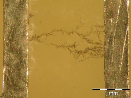
Figure 1. Short circuit caused by a Sn dendrite.
Brief introduction of the research place
The main focus of the research center – according to the Department's mission – is the investigation of material and technological aspects of physical connections between microcircuits and larger systems, where mainly knowledge on manufacturing, quality and reliability are used. Demands from the electronics industry include miniaturization, increase of integration, the increasing density of conductive layers and decreasing distances between component leads, and consequently, ever smaller areas has to be investigated, while using interdisciplinary knowledge. For this reason, the research center is equipped with special instruments capable of investigating solid phase conductive, insulating and semiconductor structures and in some cases even on liquid phases ranging from visible objects to nano sizes. So the Department has optical microscopes (Olympus SZX9 and BX51), an X-ray microscope (Dage XiDAT 6600), scanning electron microscope (FEI Inspect S50) with an energy disperse X-ray spectrometer unit (Bruker Quanta EDX), a scanning acoustic microscope (Sonix HS 1000), X-ray fluorescence spectroscopy (Spectro Midex M), and an atomic force microscope (Veeco diInnova). To perform investigations under harsh environments, different environmental chambers could be applied; a Highly Accelerated Stress Test chamber (Tabai Espec); two Thermal-Humidity Chambers (EHS-211M and Weiss, WK 180/40) (see Fig. 2.), and a Thermal Shock Chamber (Tabai Espec, TSE-11-A).
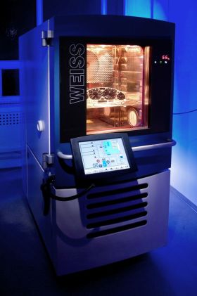
Figure 2. Thermal-Humidity Chamber
History and context of the research
Nowadays, because of the keen competition in electronic industry, customer requirements must be ranked to the first place. Therefore, ensuring the reliability and quality of electrical devices is highly important as are cost effective technologies, too. Customer requirements may vary depending on the application, but product life, quality and reliability are always a priority among them.
From the viewpoint of ECM related reliability problems, the main topics are investigations of the physical and chemical behaviors on different surface finishes and solder alloys, joints as well. Complexity of tasks has been increased by entering into force The Restriction of Hazardous Substances (RoHS) directive [1]; lead content solders have to be replaced with lead-free ones. In this context, alternative binary alloys have been examined as replacements for SnPb (traditional) solders, such as near-eutectic SnAg, SnCu, and SnZn alloys. However, ternaries (SnAgCu, SnZnAg, SnZnIn, etc.) and even quaternary alloys (SnZnAgAl, SnAgBiCu, SnInAgSb) have also been studied as candidates for lead-free solders. The reliability investigations of the lead-free solders are still very current issue among the researchers and one of the important topics is carried out about electrochemical migration (ECM) failure phenomenon [2,3].
The first theoretical explanation of the phenomenon was given in connection with the silver migration [4]. In this migration model, the dendrites are grown on the cathode by the deposition of anodically dissolved ionic constituents that are present in the conductive strips. The migrated resistive shorts occur randomly in practice and mainly under extreme conditions (i.e. high temperature and humidity). However, a number of electrical field-governed failure types are correlated with migration. A device can operate for many hundreds of hours under normal operating conditions, and then, after a short exposure to special environmental conditions, fail [4].
Later it was proven in numerous further studies that several other metals also show dendrite growth caused by ECM, i.e. Cu, Pb and Sn. Furthermore, it was also proven, that ionic contaminant has a high impact on ECM as well. Nevertheless, the presence of new lead-free based solder materials created further demands to investigate their ECM related behavior. The latest publications have also indicated the importance of this research field [5,6].
The research goal, open questions
Presently, ECM phenomenon still features many open questions, undefined reactions and processes. The existing models can not adequately describe the total process of ECM. The interpretation of the phenomenon is difficult due to the novel lead-free solder alloy systems, which are produced by various electrochemical processes.
These electrochemical processes occur in very small quantity of electrolytes (~µl), furthermore the processes are not stationary and the systems are not homogeneous either. Therefore, no equations exist to describe the phenomenon, so modeling is rather based on empirical models exist [7].
Usually, investigations are conducted in either laboratory circumstances (room temperature and humidity), or in extreme climatic conditions.
The latter one is carried out by environmental tests, which apply high temperature and humidity levels to the test structures simultaneously monitoring certain electrical parameters, such as surface insulation resistance, leakage current or voltage changing.
However, environmental tests mainly provided data about the ECM processes (fault detection) and gave very little useful information on the antecedent processes, like water condensation mechanism.
Although environmental tests can simulate the mechanism of water condensation, but minimum information could be available about physical aspects of condensation, which lead to ECM and dendrite growth [8].
Another open question that to what extent is condensation time (Mean Time To Condensation, MTTC) comparable with the time of subsequent mechanism caused by ECM and leading to short formation (dendrite growth), i.e. in certain cases condensation may not be disregarded when evaluating Mean Time To Failure (MTTF).
1. The first aim of my research was to gain a better understanding of the antecedent processes of ECM short formation. Therefore, the effect of condensation on the total failure mechanism had to be clarified. Consequently, an improvement of a novel measuring method was aimed, which provides new information about ECM behavior, for example the water condensation process during Thermal-Humidity Bias (THB) test.
2. The second aim is connected with the relation between the condensation mechanism and the ECM. Supposedly the condensation time (MTTC) strongly depends on the capillary effect and on other physical, chemical properties, such as wettability and/or water adsorption. In other words, the speed of the MTTC could be mainly determined by the type of the insulation material, hence it can be supposed that in some cases the MTTC time have huge relevance relating the MTTF. If the hypothesis will be true, than some current accelerating migration models [4] have to be modified with the MTTC.
3. Thirdly there are still many contradictory statements in the literature. One of them is about the ECM susceptibility of Pb and Cu, where a rank of ECM susceptibility was established: Ag>Pb>Cu>Sn (Silver has the highest susceptibility for ECM) [9]. The aim of this investigation is to make material choice easier considering electrical circuit design, fabrication and reliability.
4. Finally, the last aim is focused on the ECM behavior of the novel lead-free solder materials. It is known, there is a huge difference in the ECM behavior between the leaded and lead-free solder alloys [10]. Therefore, comparative investigations of different solder alloys will be done with respect to ECM. The base for comparison can be the mapping of active and passive local cells on the solder surface or structural and composition investigations of the intermetallic compound (IMC) formation.
Methodology
Although the most frequent investigating methods – like THB test – are Environmental testing methods, the so called water drop (WD) test is also widely used presently. In case of the environmental tests, the samples are stored in a climatic chamber where temperature is higher than room temperature and/or relative humidity is also high. This "aging" process is a commonly used in electronics for testing factors, which jointly or separately influence the emergence of reliability issues. Certainly, it is less suitable for qualitative observation since the process is not as fast as the water drop test. Quantitative comparison is possible when the different samples are tested under identical conditions (relative humidity, temperature, voltage) and the changes of electrical parameters are being monitored (e.g. insulation resistance or leakage current).
In the case of WD test a well-defined liquid drop (volume, concentration) is placed onto a conductive-dielectric-conductive structure and then a few volts (DC) is applied. Meanwhile, the formation of dendrites can be visually observed, the time dependence of the electrical parameter is measured and finally an average value is calculated (Mean-Time-To-Dendrite: MTTD). This is a very qualitative method; hence it does not model the real circumstances. The advantage of this method is that the electrochemical migration susceptibility of the metals can be easily and quickly established, which makes it cost-effective as well.
Additionally to the environmental and WD tests, different surface analysis methods are also required. The surface of the samples is observed with scanning electron microscope (SEM). In this case, the task is the topographical mapping of the surface (Fig. 3.); where up to 100,000 x magnifications can be reached.
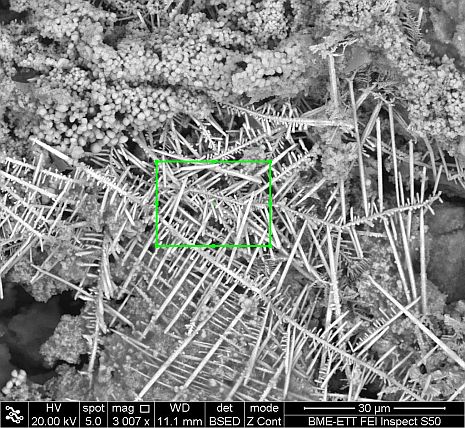
Figure 3. SEM image of a dendrite (green square= area of composition analysis)
The composition of the surface can be determined by element mapping with EDS (Energy-dispersive X-ray spectroscopy) method. EDS is a method suitable for determining the composition of materials in a given point or area, and can provide either atomic or mass ratio (Table 1).
Table 1. Composition of dendrites according to EDS method (green square).
|
Elements |
series |
[norm. wt. %] |
[norm. at. %] |
Error, wt.% (1 Sigma) |
|
Carbon |
K-series |
15.088 |
55.2388 |
2.529146 |
|
Oxygen |
K-series |
5.595984 |
15.38029 |
1.095694 |
|
Tin |
L-series |
79.31601 |
29.38091 |
2.194223 |
|
|
Sum: |
100 |
100 |
|
The X-ray Photoelectron Spectroscopy (XPS) and Scanning Auger Microscopy (SAM) are also applicable for ECM investigations. SAM is also known as Auger Electron Spectroscopy (AES) and using this technique, the sample surface is bombarded with a high energy (3 – 10 kV) primary electron beam, which results in the emission of secondary, backscattered and Auger electrons from the area of bombardment and these can be readily detected and analyzed. The secondary and backscattered electrons are used for imaging purposes similarly to scanning electron microscopy (SEM). The Auger electrons are emitted at discrete energies that are characteristic of the elements present on the sample surface. The characteristic energies of the Auger electrons are such that only the electrons from the outer 0.5 to 5 nm can escape and be detected. This makes SAM an extremely surface sensitive technique and the analysis volume is typically 106 to 108 times smaller than that excited in SEM/EDS analysis. All elements in the periodic table, except hydrogen and helium, can be detected and their concentration can be determined.
Results
My main goal was obtaining more information about the electrochemical migration processes. Therefore, I have developed an innovative monitoring system, which allows the "in-situ" and "real-time" observation of the water condensation process and the following shorting in extreme conditions (high temperature and humidity) on different surface conductor-insulator-conductor structures. The in-situ and real-time observation is possible with the following limits: -20 to +150 oC, 100% relative humidity used (see selected publications). In order to verify the measuring system, electric signal changes were measured and video recordings were taken to gather information on water condensation and the formation of dendrites.
It was observed that the condensation was more intense on metals (Fig 4.); the initial small water droplets had swollen and suddenly formed from small water "islands" into a continuous moisture film (Fig 5.), which sometimes lead across the surface of the conductor-insulator-conductor structure (water bridges).
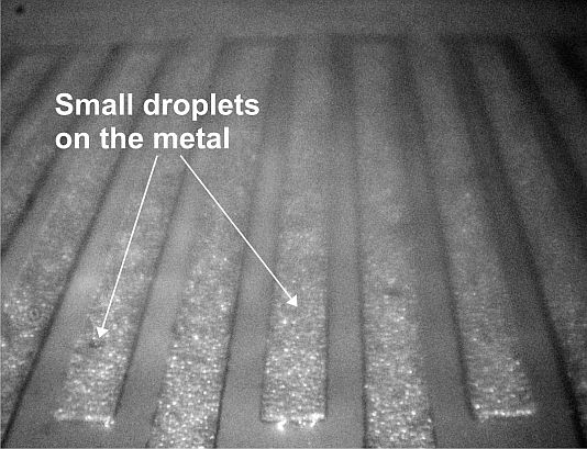
Figure 4. Start of condensation on the metal, and although humidity is less visible on the insulator, presence of condensation cores are presumed.
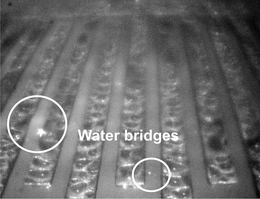
Figure 5. Appearance of water bridges due to even bigger droplets.
After this, the dendrite formation (conductive filaments) could be monitored, which led to shorts (Fig 6).
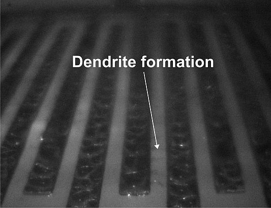
Figure 6. Dendrites formation right after the occurrence of water bridge.
This observation is important because it shows that water condensation processes taking place in the climatic chamber could have a strong influence on the short formation MTTF depending on the applied materials. However, WD test ignores MTTC time, which probably strongly varies with different conductor-insulator-conductor structures.
The so called capillary effect dominates the condensation on the insulation layers (due to the surface free energy) [11], which is the slowest process during condensation. Therefore, this impact mainly determines the MTTC, which results in water bridges (end of MTTC) and finally, dendrite formations (MTTF).
The importance of the results is that the THB test gives a better model of the total ECM process than WD test, as the latter one disregards condensation mechanism. It can be supposed that different condensation times could be detected on various conductor-dielectric-conductor systems. According to the above mentioned results, the following can be stated:
I have introduced a novel in situ and real time monitoring system, which is suitable for optical observations and simultaneous electrical parameter measurements as well during ECM processes inside climatic chambers. The monitoring system provides extended information about the ECM phenomenon, which is useful for a better understanding of the total ECM process.
It can also be supposed that the condensation time could significantly modify the time to failure time (MTTF). In order to clarify the above mentioned hypothesis, two kinds of samples were fabricated and only one parameter was changed of them: the type of the insulation layer, hence as I have mentioned the impact of the capillary effect has to be investigated relating to MTTC and MTTF.
For insulation materials, kapton® polyimide (PI) widely used in the electronic industry and the popular glass fiber-epoxy resin (FR4) were chosen.
For the investigations, an immersion silver (iAg) double comb electrode structure was designed and prepared according to IPC-B-24 standard. The iAg is still widely used in electronics for surface finishes to protect the copper base conductor.
The results of WD and THB tests were compared (see Fig 7-9.). In Figure 7, no significant differences can be observed between iAg on FR4 substrate and iAg on PI substrate and the average values are below 4 seconds.
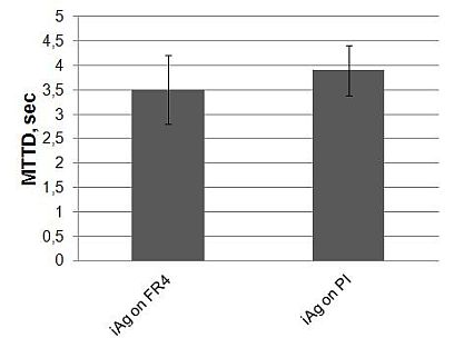
Figure 7. MTTD results of WD test on FR4 and PI substrates with iAg surface finishes (Failure criterion: 100 mVDC), without condensation effect (MTTF=MTTD).
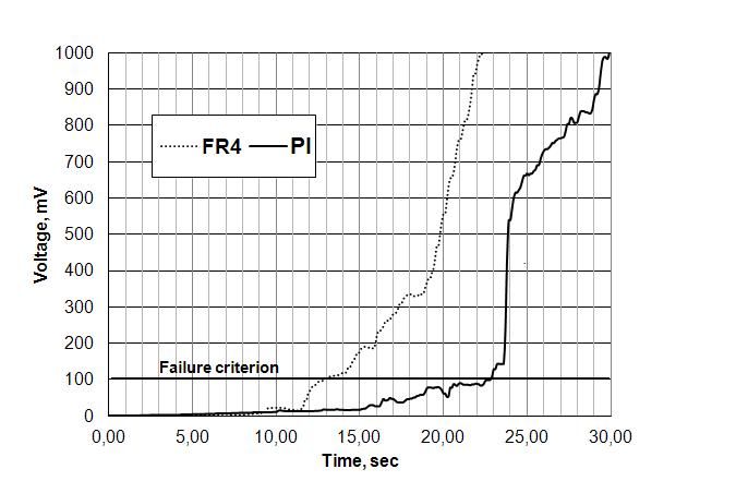
Figure 8. The MTTF difference between FR-4 and PI, with condensation effect.
In Fig. 8 a significant MTTF difference (~ 10 seconds) can be seen (see failure criterion), furthermore, the single values of FR4 and PI are also significantly high compared to the WD test results (see Fig. 9).
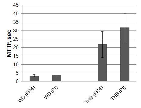
Figure 9. Time to failure for WD and THB tests (32 measurements / test).
According to the results, the following could be stated:
With the adjustment of the above mentioned in situ and real time monitoring system, it can be concluded that MTTC has a significant impact on the MTTF, if the only difference is the insulation material (FR4 vs. PI) and the conductor material is iAg.
Therefore, the existing silver ECM model have to be extended considering the above mentioned conditions:
MTTF = MTTC + MTTD
Another aim of my research work was to highlight some open questions and contradictions. A contradictory statement relates on the ECM behavior of copper and lead. Presently, an accepted ranking of the ECM susceptibility of silver, copper, tin and lead is the following: Ag>Pb>Cu>Sn (Silver is the worst). This ranking, the time to failure was correlated with the different solubility product constant of different metal hydroxides (e.g. Sn(OH)2). The recent literature considers very different values about solubility product constants of the lead(II)hydroxide. Furthermore, as in the experiments Pb containing solder alloy (i.e. not pure PB) were used, control investigations were needed. The main benefit from the investigations was that it made the choice of materials used in electrical manufacturing easier. Based on the results, the following can be stated:
I have shown that the ranking of copper and lead is not obvious, the earlier reported ranking (Ag>Pb>Cu>Sn, correlated with metal hydroxides [9]) could be modified in certain cases to: Ag>Cu>Pb>Sn. In the case of lead-containing solder alloy this can be attributed to the formation of eutectic alloy and the subsequent modified susceptibility of metal alloy anodic dissolution. In the case of copper, the oxidation state of surface influences the dissolution (see my selected publications).
Finally, I have carried out WD tests on low silver content, micro alloyed solder alloys, which are novel soldering materials. The MTTF was determined as well as the structures of dendrite and their composition was investigated. The structure and the composition of intermetallic compounds (IMC) were studied, which are in relationship with MTTF. Furthermore, the active and passive areas formed on the surface were also investigated, and the ratio of passive layers also have a significant role relating to MTTF [10].
Expected impact and further research
The electrochemical migration has become a center of focus again in the field of electronic reliability, due to the introduction of lead-free soldering. New materials are applied on various substrates with different technologies, and are operated under various environmental conditions. This itself is such a big challenge for research that it will surely determine the coming years. Susceptibility for electrochemical migration depends on many factors (not limited to): substrate materials, surface finishes, conductive path distance, operating voltage, moisture appearance mode, moisture quantity and type of contaminants and their concentration, etc. As a first step, I am going to investigate the electrochemical migration behavior of lead free solder alloys using different soldering technologies. I expect useful results for the material choice in electrical industry and in setting the optimal technological parameters during manufacturing.
Publications, references, links
Selected Publications:
Bálint Medgyes, Balázs Illés, Richárd Berenyi, Gábor Harsányi, In situ optical inspection of electrochemical migration during THB tests, JOURNAL OF MATERIALS SCIENCE-MATERIALS IN ELECTRONICS 22:(6) pp. 694-700. (2011) IF: 0.927*, WoS link, Scopus link, Full document, DOI: 10.1007/s10854-010-0198-4
Bálint Medgyes, Balázs Illés, Gábor Harsányi, Electrochemical migration behavior of Cu, Sn, Ag and Sn63/Pb37, JOURNAL OF MATERIALS SCIENCE-MATERIALS IN ELECTRONICS 23:(2) pp. 551-556. (2012) IF: 0.927**, WoS link, Scopus link, Full document, DOI: 10.1007/s10854-011-0435-5
Medgyes B, Berenyi R, Jakab L, Harsanyi G, Real-time monitoring of electrochemical migration during environmental tests, In: 32nd International Spring Seminar on Electronics Technology. Brno, Czech Republic, 2009.05.13-2009.05.17. (IEEE), pp. 1-6. WoS link, DOI: 10.1109/ISSE.2009.5207046
Medgyes B, Illés B, Contradictory Electrochemical Migration Behavior of Copper and Lead, In: 34th International Spring Seminar on Electronics Technology, ISSE2011. Tatranska Lomnica, Slovakia, 2011.05.11-2011.05.15. (IEEE), pp. 206-211, Scopus link, Full document, Document at the Publisher. DOI: 10.1109/ISSE.2011.6053579
My publications:
http://mycite.omikk.bme.hu/search/slist.php?lang=0&AuthorID=10005593
References
[1] Directive of the European Commission for the Reduction of Hazardous Substances, Directive 2000/0159 (COD) C5-487/2002, LEX 391, PE-CONS 3662/2/02 Rev 2, ENV581, CODEC 1273, 2003.
[2] D. Q. Yu, W. Jillek, E. Schmitt, Electrochemical migration of lead free solder joints, Journal of Materials Science - Materials in Electronics. 17, 229-241 (2006)
[3] J.Y Jung, S.B. Lee, H.Y. Lee, Electrochemical Migration Characteristics of Eutectic Sn-Pb Solder Alloy in NaCl and Na2SO4 Solutions, Journal of Electronic Materials. 38, 691-699 (2009)
[4] G. Harsányi, Electrochemical Processes Resulting in Migrated Short Failures in Microcircuits, IEEE Transactions on Components, Packaging, and Manufacturing Technology-Part A, 18(3), pp. 602-610 (1995)
[5] B.I. Noh, J. W. Yoon, W.S. Hong, Evaluation of Electrochemical Migration on Flexible Printed Circuit Boards with Different Surface Finishes, Journal of Electronic Materials. 38, 902-907 (2009)
[6] D. Minzari at al, Electrochemical migration of tin in electronics and microstructure of the dendrits, Corrosion Science 53, 1659–1669 (2011)
[7] S. Yang et al, Initial Stage of Silver Electrochemical Migration Degradation, Microelectronics Reliability 46, 1915–1921 (2006)
[8] Z. Sheng, M.H. Azarian, M. Pecht, Reliability of Printed Circuit Boards Processed Using No-Clean Flux Technology in Temperature Humidity Bias Conditions Device and Materials Reliability, IEEE Transactions on Device and Materials Reliability. 8, 426-434 (2008)
[9] G. Harsányi and G. Inzelt, Comparing Migratory Resistive Short Formation Abilities of Conductor Systems Applied in Advanced Interconnection Systems, Microelectronics Reliability 41, (2001)
[10] D. Q.Yu, W. Jillek, E. Schmitt, Electrochemical migration of Sn-Pb and lead free solder alloys under distilled water, Journal of Materials Science - Materials in Electronics, 17, 219-227 (2006)
[11] S. J. Krumbein, Tutorial: Electrolytic Models for Metallic Electromigration Failure Mechanisms, IEEE Transactions on Reliability, 44( 4), pp. 539-549 (I995)