|
|
BMe Research Grant |
|

Rácz Adél
BMe Research Grant - 2019
![]()
George A. Olah Doctoral School of Chemistry and Chemical Technology
MTA EK MFA, Thin Film Physics Laboratory
Supervisor: Dr. Sulyok Attila
Design and investigation of corrosion resistive SiC-rich nano-layers
Introducing the research area
Silicon-carbide (SiC) has many advantageous properties such as biocompatibility, high heat resistance, high wear resistance, good thermal conductivity and high corrosion resistance. Therefore, among others SiC is used in micro/nano-electromechanical system (MEMS/NEMS), which are operating in harsh environments e.g. in automotive and aerospace applications in combustion processes or gas turbine control [1-4]. The protection of sensors is essential. Generally the production of protective coatings requires high temperatures but certain substrates do not bear elevated temperatures. In my work, I produce SiC-rich layers by ion beam mixing at room temperature and I characterize the chemical resistance of the layers.
Brief introduction of the research place
I work with the contribution of Dr. Miklos Menyhard in MTA EK MFA, at the Thin Films Physics Laboratory. The main competence areas of our laboratory are transmission electron microscopy and different surface sensitive spectroscopic (AES, XPS) techniques.
History and context of the research
In our days, almost all functional materials from the display of smart phones, through instruments up to the engines of rockets are protected against environmental effects. These protective layers are often thin films which have advantageous properties like wear-, heat-, and corrosion-resistance and excellent hardness. For producing these layers often high temperature and high pressure processes are needed. In many cases the substrate cannot tolerate such conditions; the stable material then can be produced by a method operating far from equilibrium conditions. Among others, ion irradiation is one method which can produce even those materials at room temperature for which generally high temperatures are needed. If we irradiate a layer structure at the interfaces, then atomic mixing, or ion mixing happens. The ion-mixed layer is far from thermodynamic equilibrium; therefore chemical reactions can take place below the routine temperature. By means of ion bombardment we can control the width of boundary layer transition and the solid phases forming there. The method has been applied from the 1980s for producing thin layers of metastable compounds which have advantageous properties. Formerly, for these purposes high energy (MeV) ions were applied; the layers produced were some ten nanometers thick and located some ten nanometers far from the surface [5]. Decreasing the ion energy, thinner – some nanometers thick – layers can be created which are located close to the surface. Our laboratory gained profound experience in the investigation of the mixing of several multilayers – Si-Ge [6], Ni-C [7], Cr-Si [8], Ta-C[9], Si-C[10] - structures.
Recently, we succeeded producing SiC at room temperature in our laboratory, applying focused ion beam method (FIB) by irradiating C/Si (20-20 nm) multilayer structures with gallium ions [10]. Unfortunately, the process it is quite costly and is not feasible for irradiating macroscopic areas, thus it is not appropriate for the production of protective layers. Therefore, it is advisable to examine whether the FIB method can be replaced by other ion bombarding methods. I investigated the possibility of noble gas irradiation.
The research goals, open questions
My aim is to investigate the corrosion properties of the ion beam-mixed layers. At first, I deal with the production of the layer; I investigate the dependence of the SiC formation on the parameters of the noble gas irradiation. Therefore, I change the projectile, the fluence, the energy of the mixing ion and the layer structure. I characterize the chemical resistance of the layers produced in various ways by means of potentiodynamic corrosion test. I hope to establish a correlation between the irradiation parameters and chemical resistance.
There are various simulation techniques for the modelling of ion bombardment. They are continuously developing to provide more and more precise results within the range of wide irradiation parameters [11]. By these methods the modelling of ion mixing is limited due to their high computation-intensity. Therefore, we used simulations running faster at the cost of applying simpler descriptions with many assumptions. Such simulations are: SRIM [12] and TRIDYN [13]. Therefore, it is worth investigating the feasibility of predicting the corrosion properties of our layers by such simulation techniques with limited validity, because this would facilitate and speed up the design of the protective layer.
Another interesting area is producing SiC patterns. Applying ion irradiation through masking layer it is possible to produce SiC patterns in a single step. In this case, the compound formation and the creation of patterns take place simultaneously at room temperature; this would facilitate the standard procedures.
Methods
a. Three different C/Si multilayer structures have been irradiated by xenon and argon ions at room temperature. The applied energies were between 40–120 keV, the applied fluences between 0.25-6x10¹⁶ ion/cm2. The multilayers differed in the layer (10–20 nm) thicknesses and successions. The system was made by magnetron sputtering. I examined the SiC formation by Auger electron spectroscopy (AES) depth profiling, which could be detected by the change of the carbon and silicon Auger peaks. Fig. 1 shows this phenomenon through the Auger peak of carbon. We can see that the peak can be decomposed and is a simple sum of the SiC and graphite spectra. I calculated the amount of SiC and its in-depth distribution from the AES depth profiles.
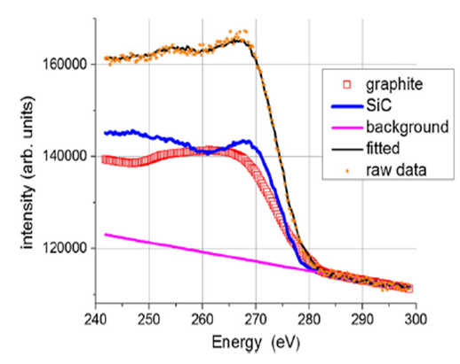
Figure 1 Auger spectra of carbon and its peak decomposition [14]]
b. For characterizing the chemical resistance of the layers, I performed potentiodynamic corrosion test in 4M KOH solution in a three-electrode cell from which I could determine the corrosion rate of the samples.
c. For predicting the effect of irradiation, I used the TRIDYN simulation software. This program describes the ion mixing of Si and C layers very well, thus we can get the in-depth distribution of the Si, C and mixing ion, from which the amount of SiC can be calculated by applying a simple rule.
d. For creating the nanostructures, I applied two different masking layers, one was a Langmuir-Blodgett film made from silica particles (diameter 590 nm), the other one was a grid with a periodicity of 2 µm. After the irradiation the mask and the non-irradiated part was removed by etching in microwave plasma and in HF/HNO3 solution. The structures were characterized by atomic force microscopy.
Results
a. The performed AES depth profiling on the irradiated samples showed that the in-depth distribution of SiC can be tuned by changing the irradiation parameters (fluence, energy) and the layer structure. Fig. 1 shows, as an example, the effect of a 6 × 10¹⁶ Ar+/cm2, 40 keV irradiation on a C/Si multilayer structure. Fig. 2a presents the AES depth profile of the non-irradiated sample, while Fig. 2b shows the profile of the irradiated one. We can see that the in-depth distribution of the non-irradiated sample exhibits C and Si layers with sharp interfaces, and that the individual thicknesses are the same. Fig. 2b shows that due to the irradiation serious changes occurred in the sample; namely, an intermixing took place. The first Si layer (below the topmost C layer) practically disappeared; it was consumed by the SiC production. On the other hand, only a part of the second Si layer was converted to SiC. This can be understood considering that the projected range of the 40 keV Ar+ is about 40 nm for this sample. [8] The last carbon layer remained more or less untouched. Considering the shape of the SiC distribution e.g. at 60 and 70 nm one can conclude that the SiC is growing from the interfaces. Fig.2c shows an irradiation where we managed to create a continuous SiC distribution.
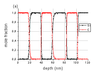
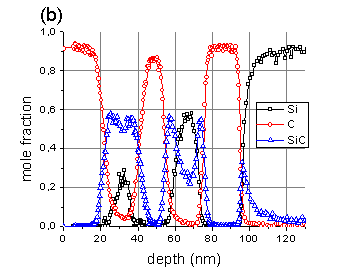
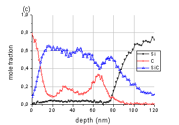
Figure 2
AES depth profiles a. non-irradiated b. irradiated (6x10¹⁶ Ar+/cm2,
40 keV)
c. irradiated (3x10¹⁶ Xe+/cm2, 120 keV)
samples
b. The corrosion tests performed on differently irradiated samples has shown that the measured corrosion current density depends on the amount of SiC and the corrosion resistance even of thin – some nanometers thick – SiC-rich layer is significantly higher than that of silicon. By introducing a new quantity, the effective areal density of SiC – calculated from the AES depth profiles – I managed to find a connection between the ion mixing and the corrosion property of the formed layer (Fig. 3). We hope that by choosing the proper irradiation conditions the chemical resistance of the layers can be tailored. [S1-S2].
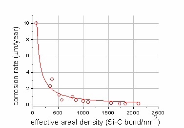
Figure 3 The corrosion rate vs. effective areal density of SiC for all measured data
c. I have shown that by applying fast and cheap simulation techniques the design of corrosion resistant layer is possible [S3]. If one wishes to tailor the corrosion resistance of a given sample; with the help of Fig. 3 one must determine and produce the SiC amount and distribution necessary to reach the desired corrosion resistance. Using an experimental approach is rather time consuming and expensive, however. To address the problem we have looked for describing the mixing process in a theoretical way. For these purposes I applied TRIDYN simulation. We knew from previous research that the TRIDYN simulation describes the mixing of C/Si system very well. Calculating the depth profiles of all irradiations, extracting the effective areal densities of SiC and plotting them as a function of the measured corrosion rates we get a curve similar to that of an Auger spectra (Fig. 4).
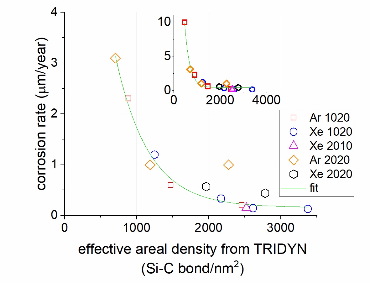
Figure 4 The corrosion rate vs. effective areal density of SiC for all measured data, inset, and enlarged y axis.
d. We can say that the creation of SiC patterns and then 3D structures therefrom was successful at room temperature. By the effect of irradiation the compound formation and patterning were completed in one step. AES depth profiling proved that in the irradiated region – i.e. the region non-protected by mask - a SiC-rich region was formed. For better understanding, the process of producing 3D structures is depicted in Fig. 5a. The AFM images of the 3D structures created by the help of LB film and lithographic grid can be seen in Figs. 5b and c. We can see that by varying the applied masks and etching procedures (etching HF/HNO3, microwave plasma) various 3D structures can be achieved. [S4].
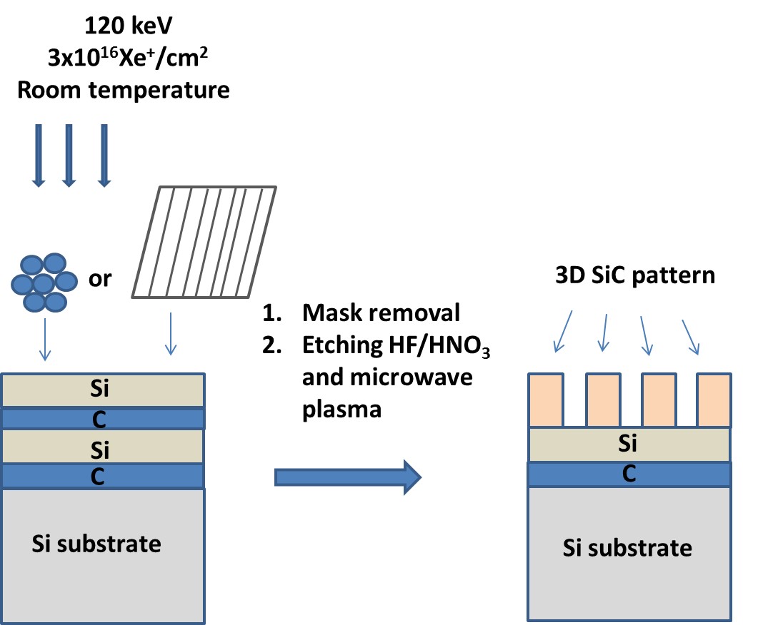
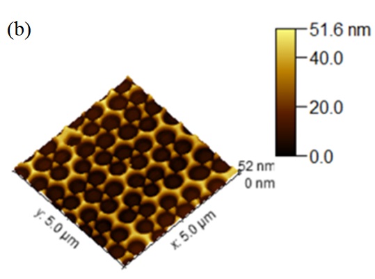
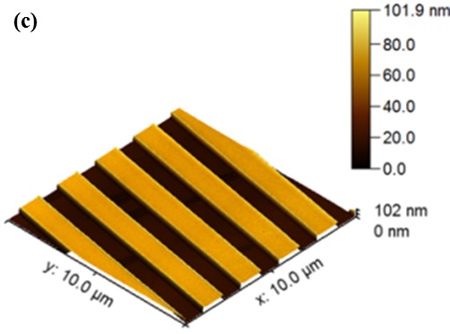
Figure 5 a. Process of producing 3D structures b. AFM image of the LB-masked sample after mask removal and one step HF/HNO3 etching and one step oxidation. c. AFM image of the grid-masked sample after mask removal and HF/HNO3 etching, oxidation and additional HF/HNO3 etching.
Expected impact and further research
It is possible that our presented method for producing SiC protective layers will be used for replacing diamond-like carbons (DLC) applied in MEMS. The importance of the research is acknowledged by two articles published in the prestigious ACS journal. In the future, I would like to investigate whether ion mixing as a procedure can be extended to the creation of other protective layers e.g. tungsten-carbide at room temperature.
Publications, references, links
List of corresponding own publications
[S1] A.S. Racz, Z. Kerner, A. Nemeth, P. Panjan, L. Peter, A. Sulyok, G. Vertesy, Z. Zolnai, M. Menyhard: Corrosion resistance of nano-sized SiC rich composite coatings produced by noble gas ion mixing, ACS Appl. Mater. Interfaces, 2017, 9 (51), pp 44892–44899. DOI: 10.1021/acsami.7b14236 IF=8.091
[S2] Rácz Adél Sarolta: Szilícium-karbidban gazdag nano-védőréteg előállítása nemesgázokkal történő ionkeveréssel, Tavaszi Szél 2017, Studies, Vol. II, pp 120–129.
[S3] A.S. Racz, M. Menyhard, Design of corrosion resistive SiC nano-layers ACS Appl. Mater. Interfaces, 2018, 10 (26), pp 22851–22856. DOI: 10.1021/acsami.8b06425 IF=8.091
[S4] A.S. Racz, D. Zambo, G. Dobrik, I. Lukacs, Z. Zolnai, A. Nemeth, P. Panjan, A. Deak, G. Battistig, M. Menyhard, Novel method for the production of SiC micro and nanopatterns, Surf. Coat. Tech., 2019, 372, pp 427–433. DOI: 10.1016/j.surfcoat.2019.05.061 IF=2.906
ΣIF=19.1
Table of links
https://en.wikipedia.org/wiki/Silicon_carbide
https://en.wikipedia.org/wiki/Nanoelectromechanical_systems
internetofthingsagenda.techtarget.com
https://en.wikipedia.org/wiki/Transmission_electron_microscopy
http://www.chem.qmul.ac.uk/surfaces/scc/scat5_2.htm
https://en.wikipedia.org/wiki/X-ray_photoelectron_spectroscopy
https://en.wikipedia.org/wiki/Thin_film
https://www.mee-inc.com/hamm/electrochemical-corrosion-testing/
http://www.hzdr.de/db/Cms?pOid=21578&pNid=0
https://en.wikipedia.org/wiki/Langmuir%E2%80%93Blodgett_film
https://www.nanoscience.com/technology/afm-technology/how-afm-works/
https://en.wikipedia.org/wiki/Diamond-like_carbon
List of references
[1] Sarro, M. Silicon carbide as a new MEMS technology. Sens. and Act. 2000, 82, 210–218.
[2] Maboudian, R.; Carraro, C.; Senesky, D.G.; Roper, C.S. Advances in silicon carbide science and technology at the micro- and nanoscales. J. Vac. Sci. Technol. A 2013, 31, 50805–50818.
[3] ) Phan, H. P.; Cheng, H. H.; Dinh, T. K.; Wood, B.; Nguyen, T. K.; Mu, F.; Kamble, H.; Vadivelu, R.; Walker, G.; Hold, L.; Iacopi, A; Haylock B.; Dao, D.V.; Lobino, M.; Suga, T.; Nguyen, N.T. Single crystalline 3C-SiC anodically bonded onto glass: an excellent platform for high temperature electronics and bio applications. ACS Appl. Mater. Interfaces 2017, 9, 27365–27371.
[4] Zorman, C.A.; Parro, R.J. Micro- and nanomechanical structures for silicon carbide MEMS and NEMS. Phys. Stat. Sol. B 2008, 245, 1404–1424.
[5] Beam-Solid Interactions: Physical Phenomena, MRS Symposia Proceedings
No. 157, edited by J. A. Knapp, P. Borgesen, and R. A. Zuhr Materials Research Society, Pittsburgh, 1989.
[6] Menyhard, M.; Barna, A.; Sulyok, A.; Järrendahl, K.; Sundgren, J.-E.; Biersack, J. P. Low Energy Ion Mixing in Si-Ge Multilayer System. Nucl. Instrum. Methods Phys. Res. Sect. B Beam Interact. Mater. At. 1994, 85 (1–4), 383–387. https://doi.org/10.1016/0168-583X(94)95849-1.
[7] Barna, Á.; Kotis, L.; Lábár, J.; Sulyok, A.; Tóth, A. L.; Menyhárd, M.; Panjan, P. Growing Imbedded Ni3C-Rich Layer with Sharp Interfaces by Means of Ion Beam Mixing of C/Ni Layers. J. Phys. Appl. Phys. 2011, 44 (12), 125405. https://doi.org/10.1088/0022-3727/44/12/125405.
[8] Barna, Á.; Kotis, L.; Lábár, J. L.; Osváth, Z.; Tóth, A. L.; Menyhárd, M.; Zalar, A.; Panjan, P. Ion Beam Mixing by Focused Ion Beam. J. Appl. Phys. 2007, 102 (5), 053513. https://doi.org/10.1063/1.2776009.
[9] Barna, Á.; Kotis, L.; Pécz, B.; Sulyok, A.; Sáfrán, G.; Tóth, A. L.; Menyhárd, M.; Kovács, A.; Savenko, A. Thin TaC Layer Produced by Ion Mixing. Surf. Coat. Technol. 2012, 206 (19–20), 3917–3922. https://doi.org/10.1016/j.surfcoat.2012.03.052.
[10] Barna, Á.; Gurban, S.; Kotis, L.; Lábár, J.; Sulyok, A.; Tóth, A. L.; Menyhárd, M.; Kovac, J.; Panjan, P. Growth of Amorphous SiC Film on Si by Means of Ion Beam Induced Mixing. Appl. Surf. Sci. 2012, 263, 367–372. https://doi.org/10.1016/j.apsusc.2012.09.063.
[11] Prskalo, A.P.; Schmauder, S.; Ziebert, C; Ye, J.; Ulrich, S. Molecular dynamics simulations of the sputtering of SiC and Si3N4, Surf. Coat. Technol. 2010, 24 (12–13), 2081-2084.
[12] SRIM Stopping and range of ions in matter by Ziegler, J. F. version SRIM, 2013 Software freely available www.srim.org
[13] Möller, W.; Posselt, M. 2001 TRIDYN_FZR User Manual FZR-317 (Dresden: Forschungzentrum Rossendorf)
[14] S. Gurban, L. Kotis, A. Pongracz, A. Sulyok, A.L. Toth, E. Vazsonyi, M. Menyhard, The chemical resistance of nano-sized SiC rich composite coating, Surf. Coat. Technol. 261 (2015) 195–200.