
|
BMe Research Grant |

|

Péter Makk
Email address
Homepage
Phone: +36 1-463-1437
Laboratory

BMe Research Grant - 2010
2nd Prize
![]()
PhD School of Physical Science
Department of Physics/Institute of Physics
Supervisor: Dr. András Halbritter
Investigation of Molecular Nanostructures
Introducing the research area
We investigate the electronic properties of atomic-sized junctions [1] created by Break Junction technique, which controls the distance of two metallic electrodes within a few pm accuracy. Our goal is to develop contacting techniques for molecules to form reproducible, well-defined contacts. The measurements are carried out at low temperatures, where several techniques can aid the understanding of the transport properties.
Brief introduction of the research place
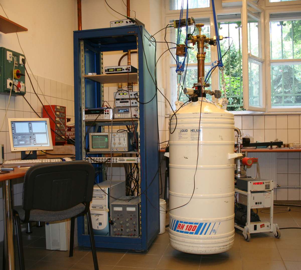
The experiments are performed at the Low Temperature Solid State Physics Laboratory of Department of Physics. The laboratory is equipped with a helium liquefier and with several cryostats and helium vessels, in which the low temperature measurements can be performed. Besides the study of atomic and molecular conductors, the lab also hosts transport and optical measurements on correlated electron systems up to high pressures and high magnetic fields.
History and context of the research
It is known that the downscaling of electronic devices will reach its limit in a short time and conventional techniques cannot be further improved. The biggest challenge in solid-state physics in our time is to find future technologies capable of replacing the current ones.
The idea that a single atom or molecule can function as the active part of an electrical unit is more than 35 years old [2], however, experiments have only turned this vision into a promising alternative during the last decade.
Several interesting results, such as the formation of atomic chains[3], the contacting of individual molecules[4,5,6,7], the conductance switching of molecular junctions by mechanical tuning [8], light irradiation [9] and in-situ chemical reactions [10] have been reported. Memory cells [11] and even single molecule transistors have been realized [12], where large currents can be switched by putting a single electron charge on a molecule.
Although these results hold the promise for various future applications (from nanosensors to molecular memories), the reliability and reproducibility of these devices are not yet resolved. Our group conducts research on single-atom as well as molecule junctions searching for reliable contacting techniques and developing widely usable characterization methods.
Aim of the research
Our long term goal of building functional single-molecule electronic devices necessitates the development of reliable characterization techniques. Usually single molecule devices – due to their extremely small sizes – cannot be observed directly, and all the information about the device is obtained from indirect electronic measurements. However, there are several methods available for getting additional information from current and voltage measurements.
In many cases, even the most fundamental question, i.e. whether or not a single piece of a chosen molecule is contacted is difficult to answer, and obtaining more detailed information about the conformation of the molecular arrangement is almost impossible. Although, a wide of range of possibilities in the nanoscale chemical design of molecular structures is already available, the reproducibility and the stability of these devices are yet unsolved, critical issues.
 |
|
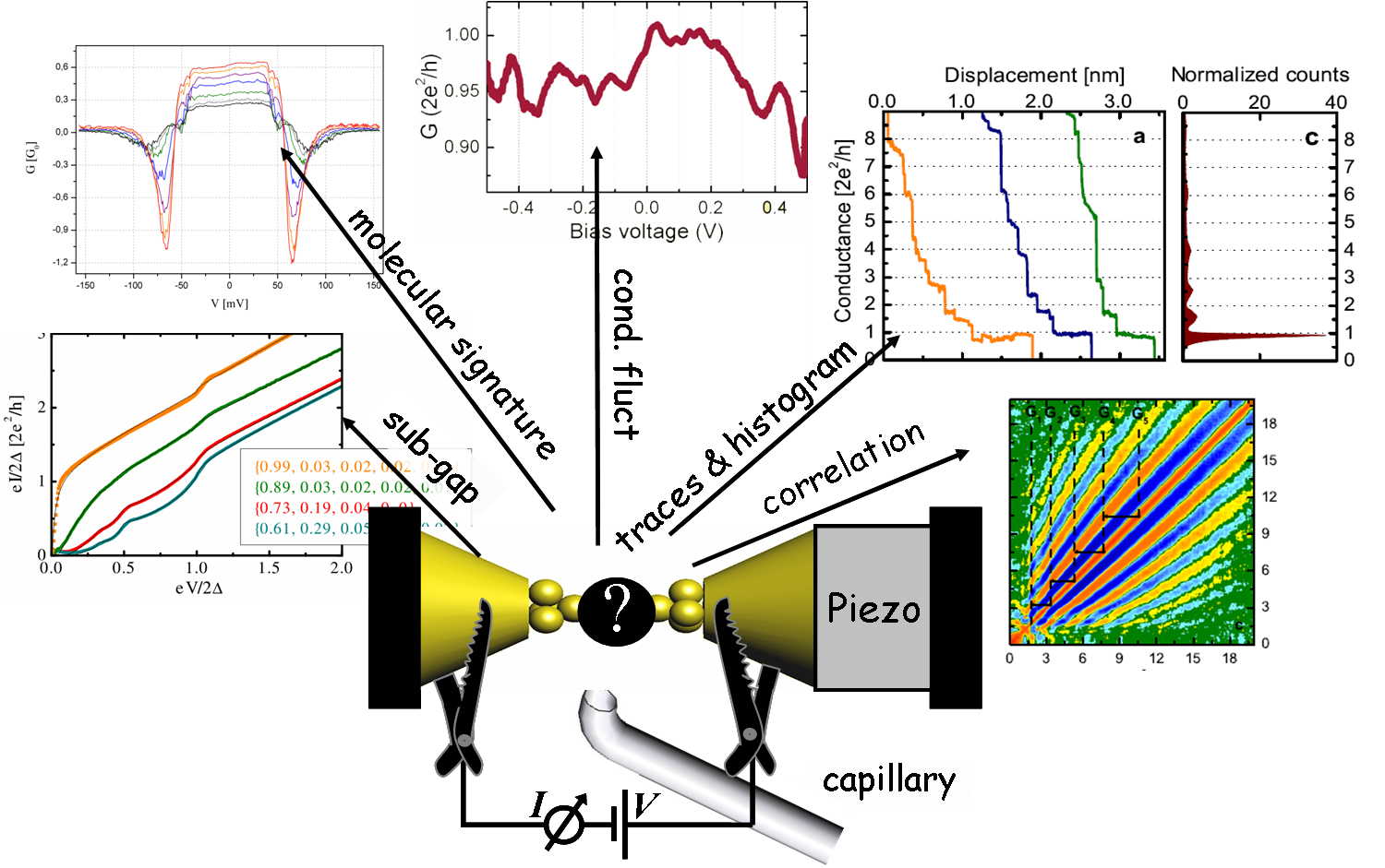
Atomic junctions made by the break-junction method. Although the contact cannot be directly observed, there are several methods that helps deeper understanding of the nanoscale behavior. |
The main goal of our measurements is to develop reliable methods for contacting single molecules and construct proper characterization tools for these devices. A summary of these methods are presented on the figure above and discussed later on.
Methods
|
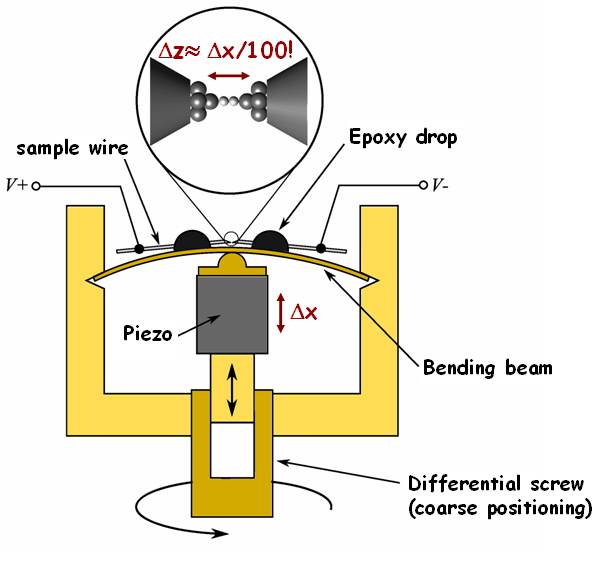
Break Junction method
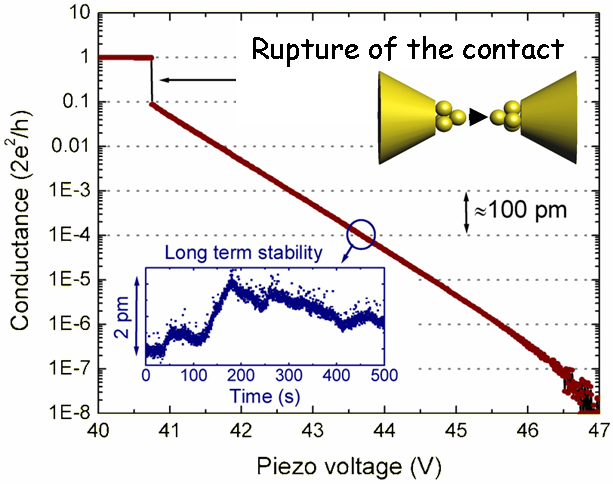
In our experiments, we form atomic contacts with Mechanically Controllable Break Junction technique (MCBJ), where few-atom configurations are created by breaking a metallic wire. We glue the wires on a metallic substrate and tune the contact size by bending the substrate with a piezo element. The high transmission ratio between the movement of the piezo element and the electrode separation enables the fine tuning of the contact size. Measuring at low temperatures
The BJ system is built in a sample holder, which is placed in a liquid helium transport vessel and cooled down to 4K, where low temperature adds extreme stability to the setup and enables tuning of the electrode separation on the picometer scale.
|
|
|
|
Schematic view of the MCBJ setup |
The sample and the bending setup is situated in the vacuum chamber of the sample holder to assure cryogenic vacuum after the system cools down. If freshly broken there, cleanness of contact surfaces can be guarantied for a long time, and a big variety of materials – including strongly reactive metals – can be applied as electrodes.
|
|
Left: Measurement setup. The helium dewar with the sample holder is suspended to damp vibrations. Right: Tunneling calibration measurements on gold contact. The exponential behaviour of the tunnel current as a function of electrode distance can be observed through 6 orders of magnitude. The inset shows stability of the system. |
Introducing the molecules
Molecules are admitted to the sample space in small doses, and they are directed to the close vicinity of the junction in the cryogenic part of the setup through a capillary tube. The molecules – if selected properly – can bind chemically to the electrodes forming a molecular bridge.
Conductance histogram
The atomic granularity of matter is clearly manifested during the rupture of a metallic wire. As the narrowing of the wire reaches atomic dimensions, the continuous change of conductance is replaced by discrete jumps reflecting the rearrangements of atoms in the smallest cross section. If the contact rupture is repeated several times the evolution of the conductance features similarities in the general character with differences only in the details [1].
|
|
|
|
|
|
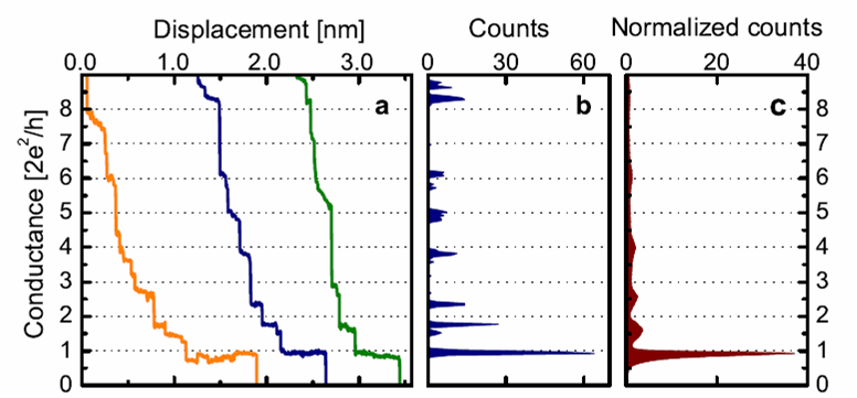
Left: Individual conductance traces for Au; Middle: Conductance histogram for these curves; Right: Histogram for all the traces for the measurement. |
|
To statistically analyze this process conductance histograms are constructed from individual conductance vs. electrode separation traces. The conductance histogram shows the most probable conductance values of stable atomic or molecular configurations reflected by peaks in the histogram.
Theoretical description of the conductance at atomic scale
After identifying the statistically relevant configurations, properties of individual configurations can be studied by fixing the electrode separation. The size of these junctions are comparable to the wavelength of electrons, therefore quantum mechanical effects are becoming dominant. Analyzing these effects can help us get more insight into the transport properties of the junction.
|
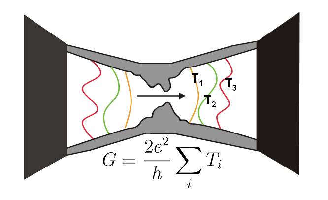
In mesoscopic physics, nanosized junctions can be described with a set of transmission coefficients, sometimes referred to as the "Mesoscopic PIN-code" [1]. These transmission coefficients represent the probabilities of transmission of electron waves through the junction. The Landauer formula, shown in the figure to the left, links the sample's conductance with microscopic, electron-structure-based properties of the material [13]. It can be seen, that these coefficients cannot be determined individually from simple conductance measurements, just their sum. |
|
Model of atomic contacts. Electron waves are transmitted through the constriction with probability Ti. |
|
There are some methods that can be used to determine these coefficients, e.g. conductance fluctuation effects coming from random interference of electron waves are hallmark of quantum mechanical behavior, and their size is related to the transmission coefficients [14, 15].
Moreover, superconducting electrodes provide us with the unique opportunity of determining all the coefficients with high precision [13, M2] (see later).
Results
We have performed measurements on metallic contacts and single molecular junctions. As understanding both from experimental and theoretical point of view is quite challenging even for simple molecular junctions, first we performed measurements with the simplest possible molecular junction, hydrogen between metallic electrodes. In our recent experiments we are trying to extend these measurements on more complex molecules.
Correlation analysis
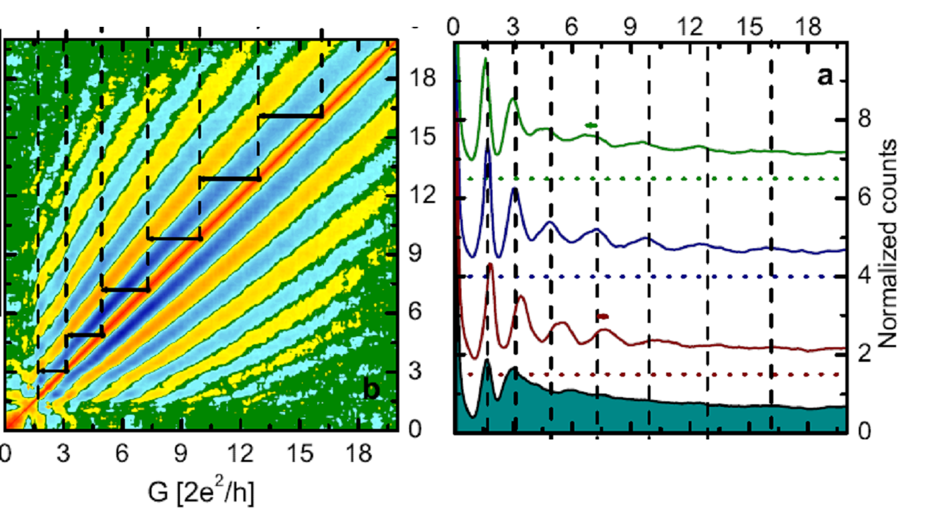
Conductance histogram technique is widely applied in the field of molecular electronics to identify single atomic or molecular structures. However, conventional conductance histograms – measuring statistical averages – can only provide limited information about the studied nanostructures. Therefore, we have developed a novel statistical method based on the 2D cross-correlation analysis of conductance traces [M4] that is capable of resolving several features of nanocontact formation otherwise completely hidden in traditional conductance histograms. It can identify correlated or anti-correlated occurrence of different junction configurations. This analysis has demonstrated robust structures in the correlation diagram for Ni, Fe and V, which we have attributed to the atom by atom narrowing of the minimal cross section of the wire, in contrast to the unordered rupture of Au junctions.
|
|
|
|
|
|
Left: Correlation diagram of Ni nanojunctions. Right: Original conductance histogram (bottom) and histograms with several features revealed by the correlation analysis. For details see M4. |
|
Subgap spectroscopy on metallic systems and molecular junctions
We have investigated superconducting metallic junctions with subgap method. By measuring and fitting I-V curves on large amount of different junctions, the statistical evolution of transmission coefficients can be tracked as a function of the junction's conductance. This also provides us with a solid basis for comparing our later results on molecular junctions.
We investigated the interaction of hydrogen molecules with superconducting electrodes [M1, M2]. We applied first the superconducting subgap method for measuring the transmission coefficients of molecular nanojunctions. For Nb and Ta we showed that unlike the dramatic changes of mechanical properties in the junction’s neighborhood caused by their interaction with hydrogen, which is possibly dissolved to the electrodes, electronic properties do not change and remain dominated by the conductance properties of Nb and Ta.
|
|
|
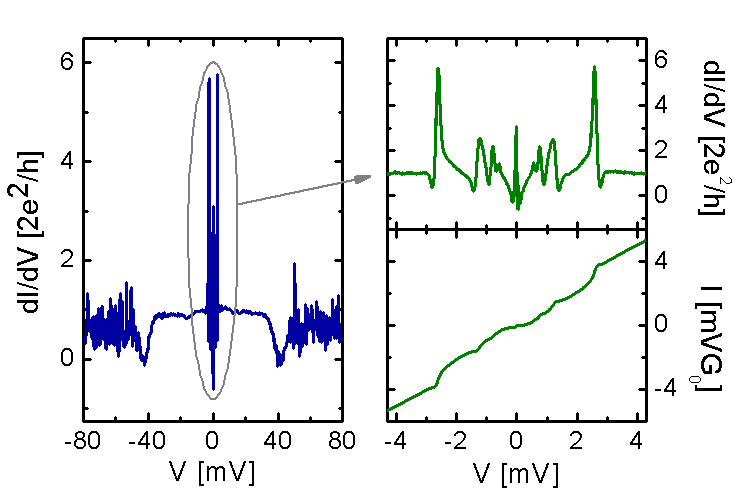
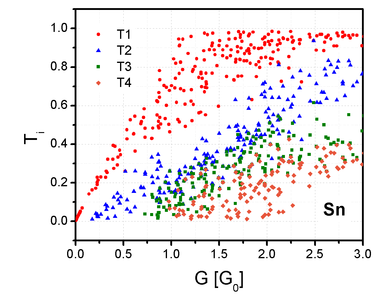
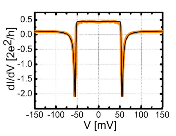
Left: dI/dv curves for Nb nanojunctions. Both the elastic (subgap) and the inelastic excitations (negative differential conductance) can be observed. On the right panel the subgap structure is enlarged in green. Right: Transmission probabilities vs. conductance for the first four channels for Sn nanojunctions. |
|
Signature of molecular junctions – Negative differential resistance
We have shown that both the elastic (like the transmission properties from subgap features) and the inelastic excitations of molecular nanojunctions can be determined from a singe I-V characteristics measurement [M3]. Junctions frequently exhibit negative differential conductance due to the inelastic excitation of a strongly bound molecule to large number of energetically similar loosely bound states. For this phenomenon we have also developed a theoretical model. |
|
Negative differential conductance on Au-H2 junctions |
|
|
|
|
|
|
|
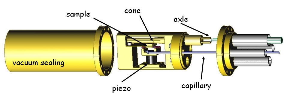
Sample holder developed for dosing molecules |
|
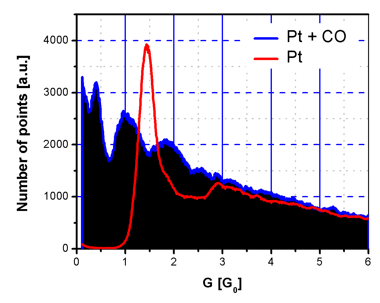
We have developed a sample holder with a heated capillary and with a more sophisticated vacuum system to avoid contamination (protective cryogenic vacuum shield disappears with heating). This system can be used to deposit molecules larger than hydrogen, which condensate at 4K. So far, we have performed test measurements on the Pt-CO system already known from the literature [16], and presently we conduct measurements on small molecules and superconducting electrodes.
|
|
|
|
|
|
Conductance histogram for pure Pt (red) and for Pt-CO system (blue). |
|
Expected impact and further research
Nanoscale devices exhibit behaviours fundamentally different from macroscopic objects'. To understand this completely new behavior we need well-prepared model systems, where we can investigate these novel properties in detail. Our main goal is to find such thoroughly understood reference systems, which could later act as measurement standards in the field of molecular electronics.
We continue our studies with the detailed investigation of interaction of simple molecular gases with various metallic electrodes. Well-defined molecular configurations will be compared with ab initio calculations and will be studied also at room temperature. Later work will focus on complex organic molecules with predefined properties and functional side groups suitable for switching or sensing devices.
Publications, references, links
Publications
[M1] A. Halbritter, Sz. Csonka, P. Makk, Gy. Mihály: Interaction of hydrogen with metallic nanojunctions. Journal of Physics: Conference Series 61, 214–218 (2007)
[M2] P. Makk, Sz. Csonka and A. Halbritter: Effect of hydrogen molecules on the electronic transport through atomic-sized metallic junctions in the superconducting state. Phys. Rev. B. 78, 045414 (2008)
[M3] A. Halbritter, P. Makk, Sz. Csonka and Gy. Mihály: Huge negative differential conductance in Au-H2 molecular nanojunctions. Phys. Rev. B. 77, 075402 (2008)
[M4] A. Halbritter, P. Makk, Sz. Mackowiak, Sz. Csonka, M. Wawrzyniak, J. Martinek: Atom by atom narrowing of transition metal nanowires resolved by 2D correlation analysis. arXiv:1006.1811v1, submitted to Nature Nanotechnology
Links
Nanoelectronics group of the University of Basel
Atomic and molecular conductors group in Leiden
Centre for Nanoscale Dynamics and Mathematical Modelling in Lancaster
Other references
Molecular electronics on wikipedia
Lectures of Supriyo Datta on moleceular electronics
Thomas Ihn: Semiconductor Nanostructures. ISBN13: 9780199534425. Oxford University Press, 2010
References
[1] N. Agräit, A. L. Yeyati, J. M. van Ruitenbeek: Quantum properties of atomic-sized conductors Phys. Rep. 377, 81–279 (2003).
[2] A. Aviram and M.A. Ratner: Molecular Rectifiers. Chem. Phys. Lett. 29, 277 (1974)
[3] A.I. Yanson, G. Rubio Bollinger, H. E. van den Brom, N. Agräit and J. M. van Ruitenbeek: Formation and manipulation of a metallic wire of single gold atoms Nature 395, 783–785 (1998).
[4] R.H.M. Smit, et al.: Measurement of the conductance of a hydrogen molecule Nature 419, 906–909 (2002).
[5] B. Xu, N. J. Tao: Measurement of single-molecule resistance by repeated formation of molecular junctions Science 301 1221–1223 (2003)
[6] L. Venkataraman, Jennifer E. Klare, Colin Nuckolls, Mark S. Hybertsen, and Michael L. Steigerwald: Dependence of singlemolecule junction conductance on molecular conformation Nature 442, 904–907 (2006).
[7] S. Wu, et al.: Molecular junctions based on aromatic coupling Nature Nanotechnology 3, 569–574 (2008).
[8] S. Y. Quek, et al:, Mechanically controlled binary conductance switching of a single-molecule junction Nature Nanotechnology 4, 230–234 (2009)
[9] S. J. van der Molen, et al.: Light-controlled conductance switching of ordered metal−molecule−metal devices Nano Lett. 9 76–80 (2009)
[10] J. Liao, et al.: Cyclic conductance switching in networks of redox-active molecular junctions Nano Lett., 10 759–764 (2010)
[11] Jonathan E. Green et al.: A 160-kilobit molecular electronic memory patterned at 1011 bits per square centimeter Nature 445, 414–417 (2007)
[12] H. Park, et al.: Nano-mechanical oscillations in a single-C60 transistor. Nature 407, 57–60 (2000)
[13] E. Scheer et al.: The signature of chemical valence in the electrical conduction through a single-atom contact Nature 394, 154–157 (1998).
[14] B. Ludoph, M.H. Devoret, D. Esteve, C. Urbina and J.M. van Ruitenbeek: Evidence for saturation of channel transmission from conductance fluctuations in atomic-size point contacts Phys. Rev. Lett., 82, 1530-3 (1999)
[15] A. Halbritter, et al.: Quantum interference structures in the conductance plateaus of gold nanojunctions
Phys. Rev. B. 69, 121411(R) (2004)
[16] O. Tal, et al.: Molecular signature of highly conductive metal-molecule-metal junctionsPhys. Rev. B 80, 085427 (2009)